Download
1 / 28
310 likes | 449 Views
Scaling of the performance of carbon nanotube transistors. S. Heinze 1 , M. Radosavljevi ć 2 , J. Tersoff 3 , and Ph. Avouris 3. 1 Institute of Applied Physics, University of Hamburg, Germany 2 Novel Device Group, Intel Corporation, Hillsboro, OR

E N D
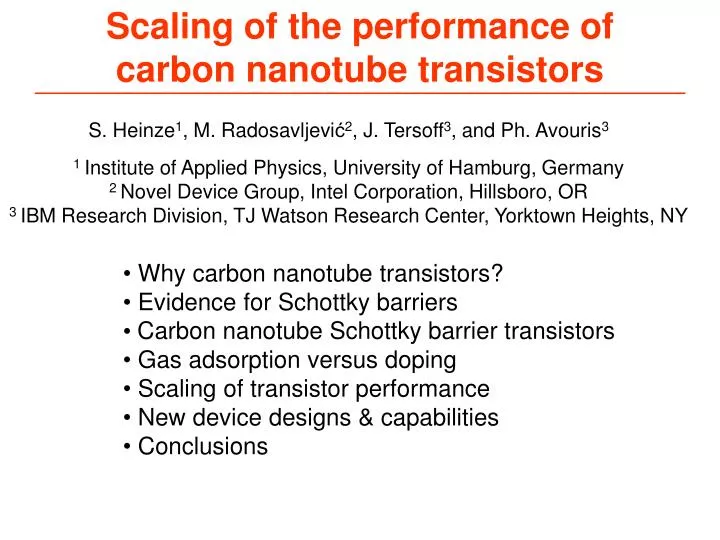
Scaling of the performance ofcarbon nanotube transistors S. Heinze1, M. Radosavljević2, J. Tersoff3, and Ph. Avouris3 1 Institute of Applied Physics, University of Hamburg, Germany 2 Novel Device Group, Intel Corporation, Hillsboro, OR 3 IBM Research Division, TJ Watson Research Center, Yorktown Heights, NY • Why carbon nanotube transistors? • Evidence for Schottky barriers • Carbon nanotube Schottky barrier transistors • Gas adsorption versus doping • Scaling of transistor performance • New device designs & capabilities • Conclusions
Carbon nanotube field-effect transistors comparable with Si MOS-FETs • favorable device characteristics • Nanotube FETs with top gates: • turn-on gate voltage is about 1V S. J. Wind et al., Appl. Phys. Lett. 80, 3817 (2002).
Evidence for Schottky barriers:scanned gate microscopy at contacts (a) (b) Vtip = -2V map transport current as a function of moving, charged AFM tip current increase when gating the source junction barrier thinning. M. Freitag et al., Appl. Phys. Lett. 79, 3326 (2001).
Evidence for Schottky barriers:ambipolar conduction in SWNTs Bottom gate CNFETs with Ti contacts annealed; conversion from p-type to ambipolar conductance R. Martel et al., PRL 87, 256805 (2001).
Evidence for Schottky barriers: Influence of the contacts for CNFETs -500 Vg=-1.5V to 0V 0.5V steps -400 NT -300 Current [nA] -200 -100 0 0.0 -0.5 -1.0 -1.5 Drain Voltage [V] Vd Vs = 0 Switching S & D changes:– Slope by factor of 2– ON-state by factor of 5 Vs = 0 Vd not due to bulk, it is a contact effect Vg M.Radosavljević et al. -6 10 -7 L=300nm tox=5nm 10 -8 10 -9 10 Current [A] -10 10 -11 10 Vd=-0.9V to -0.5V 0.2V steps -12 10 -13 10 -2.0 -1.0 0.0 1.0 Gate Voltage [V]
Conventional vs. Schottky barrier FET Conventional Transistor Schottky Barrier Transistor ambipolar Characteristic dNT=1.4nm Eg~0.6eV Typical SBs for NTs ~ 0.3eV p-type Characteristic
Transmission through Schottky barrier WKB approximation + single NTband: Landauer-Büttiker formula for current:
Self-consistent SB-transistor modelfor needle-like contact Electrostatic potential: Charge on the nanotube: Solution by self-consistency cycle Gate • Cylindrical gate at RGate • Metal electrode of NT diameter • Analytic electrostatic kernel G • Test of approximations for NT Metal
Needle-like contact:conductance vs. gate voltage Gate Metal NT Ideal sharp Metal-NT Contact turn-on voltage ~ Eg/2
Carbon nanotube transistors with planar gates Calculated NT-potential Electrostatic Potential Conductance Modulation • Solve a 2D boundary value problem Vext(x) • Local approximation for potential from NT charge
Influence of the contact geometry Gate Metal NT Scaled Characteristics PRL 89, 106801 (2002)
Increase of O2 Gas adsorption vs. doping:Experimental observations Gas Adsorption (O2) Doping with Potassium Increase of Potassium V. Derycke et al., APL 80, 2773 (2002).
Uniform doping:Experiment vs. SB model Gate Metal NT Increase of Potassium Needle-Contact Model Doping with Potassium
Uniform doping of nanotube Gate Metal NT n-doped at 510-4 e/atom Calculated Doping Characteristics
Uniform doping of nanotube Gate Metal NT n-doped at 110-3 e/atom Calculated Doping Characteristics
Gas adsorption: Experiment vs. SB model Gate Metal NT Gas Adsorption (O2) Needle-Contact Model Increase of O2
Gas adsorption:Change in metal workfunction Gate Metal workfunction increased by 0.2eV Calculated Gas Adsorption Characteristics Metal NT
How does the performance of Schottky barrier CNFETs scale? ultra-thin oxide CNFETs: Scaling law with oxide thickness? Why is the thermal limit of 60 mV/decade not reached? J. Appenzeller et al., PRL 89, 126801 (2002).
Turn-on vs oxide thickness for bottom gate SB-CNFETs Device geometry Vscale~ sqrt(tox)
Analytic model for thin sheet contact Potential near the Edge:
Analytic model applied to bottom gate SB-CNFETs Single, empirical factor for bottom gate devices
Scaling of turn-on performance of CNFETs with oxide thickness Analytic Model Largest improvements by optimization of the contact geometry PRB 68, 235418 (2003)
Scaling of drain voltage for ultra-thin oxide CNFETs? Minimal Current (OFF-current) rises with lower oxide thickness Top Electrode 0.1 120 0.2 0.3 80 Height (nm) 0.4 0.3 t =30nm ox 40 Drain=0.5V Source Nanotube t =2nm ox 0.0 0.9 0 Bottom Gate=1V -0.3 Energy (eV) 0 100 200 300 400 Source Length (nm) -0.6 • independent barriers – • one controlled by Vg, the other by Vd–Vg • identical (and minimal) hole/electron current at Vg = Vd–Vg Vd = 2Vg -0.9 V =+0.8V, V =+0.4V Drain drain gate Ultra-thin oxide: turn-on voltage ~ Vd -1.2 0 100 200 300 400 Position along Nanotube (nm)
Effect of drain voltage for ultra-thin oxide CNFET Bottom-gate: tox=2nm exponential increase of OFF current with Vd
Scaling of drain voltage: model vs. experiment tox=2nm APL 83, 2435 (2003)
OFF state problem for transistor light emission device Infrared light emission from a SWNT: J. Misewich et al., Science 300, 783 (2003).
Asymmetric device design to solve OFF state problem • Symmetric CNFET (tox=2nm) • unfavorable OFF state Asymmetric CNFET low OFF current & p- and n-type device for Vd<0 and Vd>0 APL 83, 5038 (2003)
Conclusions CN Transistors competetive with Si MOSFETs, however: • Transistor action in CNFETs due to Schottky barriers • ambipolar transfer characteristic (I vs Vg) • Nanoscale features of contacts are essential • Gas adsorption modifies band line-up at the contact • Scaling in turn-on regime with sqrt(tox) • Scaling of drain voltage at ultra-thin oxides necessary • New device physics: light emission device • New device designs may be favorable