Download
1 / 17
200 likes | 594 Views
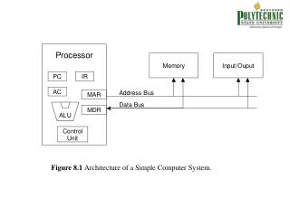
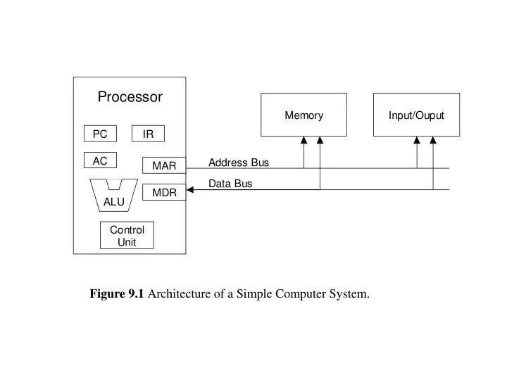
Figure 9.1 Architecture of a Simple Computer System. Figure 9.2 Simple m P 3 Computer Instruction Format. Figure 9.3 Basic m P 3 Computer Instructions. Assembly Language MachineLanguage LOAD B 0211 ADD C 0012 STORE A 0110. Figure 9.4 Example Computer Program for A = B + C.

E N D
Assembly Language MachineLanguageLOAD B 0211ADD C 0012STORE A 0110 Figure 9.4 Example Computer Program for A = B + C.
Figure 9.6 Detailed View of Fetch, Decode, and Execute for the mP 3 Computer Design.
Figure 9.7 Datapath used for the mP 3 Computer Design. Values shown after applying reset.
Figure 9.8 Register transfers in the ADD instruction’s Fetch State.
Figure 9.9 Register transfers in the ADD instruction’s Decode State.
Figure 9.10 Register transfers in the ADD instruction’s Execute State.
-- Simple Computer Model Scomp.vhd LIBRARY IEEE; USEIEEE.STD_LOGIC_1164.ALL; USEIEEE.STD_LOGIC_ARITH.ALL; USE IEEE.STD_LOGIC_UNSIGNED.ALL; LIBRARY altera_mf; USEaltera_mf.altera_mf_components.ALL; ENTITY SCOMP IS PORT( clock, reset : INSTD_LOGIC; program_counter_out : OUTSTD_LOGIC_VECTOR( 7 DOWNTO 0 ); register_AC_out : OUT STD_LOGIC_VECTOR(15 DOWNTO 0 ); memory_data_register_out : OUT STD_LOGIC_VECTOR(15 DOWNTO 0 )); memory_address_register_out : OUT STD_LOGIC_VECTOR(7 DOWNTO 0 ); memory_write_out : OUT STD_LOGIC); END SCOMP; ARCHITECTURE a OF scomp IS TYPE STATE_TYPE IS ( reset_pc, fetch, decode, execute_add, execute_load, execute_store, execute_store2, execute_jump ); SIGNAL state: STATE_TYPE; SIGNAL instruction_register, memory_data_register : STD_LOGIC_VECTOR(15 DOWNTO 0 ); SIGNAL register_AC : STD_LOGIC_VECTOR(15 DOWNTO 0 ); SIGNAL program_counter : STD_LOGIC_VECTOR( 7 DOWNTO 0 ); SIGNAL memory_address_register : STD_LOGIC_VECTOR( 7 DOWNTO 0 ); SIGNAL memory_write : STD_LOGIC; BEGIN -- Use Altsyncram function for computer's memory (256 16-bit words) memory: altsyncram GENERIC MAP ( operation_mode => "SINGLE_PORT", width_a => 16, widthad_a => 8, lpm_type => "altsyncram", outdata_reg_a => "UNREGISTERED", -- Reads in mif file for initial program and data values init_file => "program.mif", intended_device_family => "Cyclone") PORT MAP (wren_a => memory_write, clock0 => clock, address_a =>memory_address_register, data_a => Register_AC, q_a => memory_data_register ); -- Output major signals for simulation program_counter_out <= program_counter; register_AC_out <= register_AC; memory_data_register_out <= memory_data_register; memory_address_register_out <= memory_address_register;
PROCESS ( CLOCK, RESET ) BEGIN IF reset = '1' THEN state <= reset_pc; ELSIF clock'EVENTAND clock = '1' THEN CASE state IS -- reset the computer, need to clear some registers WHEN reset_pc => program_counter <= "00000000"; register_AC <= "0000000000000000"; state <= fetch; -- Fetch instruction from memory and add 1 to PC WHEN fetch => instruction_register <= memory_data_register; program_counter <= program_counter + 1; state <= decode; -- Decode instruction and send out address of any data operands WHEN decode => CASE instruction_register( 15 DOWNTO 8 ) IS WHEN "00000000" => state <= execute_add; WHEN "00000001" => state <= execute_store; WHEN "00000010" => state <= execute_load; WHEN "00000011" => state <= execute_jump; WHENOTHERS => state <= fetch; ENDCASE;
-- Execute the ADD instruction WHEN execute_add => register_ac <= register_ac + memory_data_register; state <= fetch; -- Execute the STORE instruction -- (needs two clock cycles for memory write and fetch mem setup) WHEN execute_store => -- write register_A to memory, enable memory write -- load memory address and data registers for memory write state <= execute_store2; --finish memory write operation and load memory registers --for next fetch memory read operation WHEN execute_store2 => state <= fetch; -- Execute the LOAD instruction WHEN execute_load => register_ac <= memory_data_register; state <= fetch; -- Execute the JUMP instruction WHEN execute_jump => program_counter <= instruction_register( 7 DOWNTO 0 ); state <= fetch; WHENOTHERS => state <= fetch; ENDCASE; ENDIF; ENDPROCESS;
-- memory address register is already inside synchronous memory unit -- need to load its value based on current state -- (no second register is used - not inside a process here) WITH state SELECT memory_address_register <= "00000000" WHEN reset_pc, program_counter WHEN fetch, instruction_register(7 DOWNTO 0) WHEN decode, program_counter WHEN execute_add, instruction_register(7 DOWNTO 0) WHEN execute_store, program_counter WHEN execute_store2, program_counter WHEN execute_load, instruction_register(7 DOWNTO 0) WHEN execute_jump; WITH state SELECT memory_write <= '1' WHEN execute_store, '0' WHEN Others; END a;
DEPTH = 256; % Memory depth and width are required % WIDTH = 16; % Enter a decimal number % ADDRESS_RADIX = HEX; % Address and value radixes are optional % DATA_RADIX = HEX; % Enter BIN, DEC, HEX, or OCT; unless % % otherwise specified, radixes = HEX % -- Specify values for addresses, which can be single address or range CONTENT BEGIN [00..FF] : 0000; % Range--Every address from 00 to FF = 0000 (Default) % 00 : 0210; % LOAD AC with MEM(10) % 01 : 0011; % ADD MEM(11) to AC % 02 : 0112; % STORE AC in MEM(12) % 03 : 0212; % LOAD AC with MEM(12) check for new value of FFFF % 04 : 0304; % JUMP to 04 (loop forever) % 10 : AAAA; % Data Value of B % 11 : 5555; % Data Value of C% 12 : 0000; % Data Value of A - should be FFFF after running program % END ; Figure 9.12 MIF file containg mP Computer Program.
Figure 9.14 Simulation display of mP 3 Computer Memory showing result stored in memory