Download
1 / 53
540 likes | 619 Views
Learn about synchronous and asynchronous counters, constructing and connecting counters, various counter types, decoding schemes, shift registers, and troubleshooting techniques.

E N D
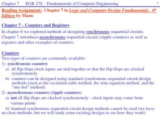
Chap. 7 Counters and Registers • Chapter Outcomes (Objectives) • Describe the operation and characteristics of synchronous and asynchronous counters. • Construct counters with MOD numbers less than 2N. • Construct both up and down counters. • Connect multistage counters. • Analyze and evaluate various types of counters. • Design arbitrary-sequence synchronous counters. • Describe several schemes used to decode different types of counters. • Describe counter circuits using different levels of abstraction in HDL. • Construct shift register counters. • Explain the operation of various types of IC registers. • Describe shift registers and shift register counters using HDL. • Apply troubleshooting techniques used for combinational logic systems to troubleshoot sequential logic systems.
Chap. 7 Counters and Registers • Introduction • Main topics in the Chap. 7 • How FFs and logic gates can be combined to produce different types of counters and registers • Divided into 2 parts • Part I : principles of counter operation, various counter circuit arrangement, and representative IC counters • Part II : counter application, types of IC register, and troubleshooting • 7-1 Asynchronous(Ripple) Counters • Asynchronous Counter : Fig. 7-1 • The FFs do not change states in exact synchronism with the applied clock pulses • Ripple Counter • The FFs respond one after another in a kind of rippling effect • The terms asynchronous counter and ripple counter interchangeably • Signal Flow(in Fig. 7-1) • Left-to-Right : Conventional signal flow • Right-to Left : • FF A(rightmost) = LSB, FF D(leftmost) = MSB We’ll break left-to-right convention, especially in counter diagrams
Asynch Synch Fig. 7-1 : Four-bit Asynchronous (ripple) Counter
Exam. 7-1)Some time later the clock pulses are removed, and the counter FFs read 0011. How many clock pulses have occurred? • 3 + 16 = 19 + 16 = 35 + 16 = 51 ….. • Mod Number = 2N( N : number of FF ) • Number of different states • Fig. 7-1 : MOD-16 ripple counter ( 0000 1111) • Exam. 7-2)The counter must be able to count as many as one thousand items. How many FFs are required ? • 10 FFs : 0 1023 ( 1001 1023은 필요 없음 ) • Frequency Division • For any counter, the output from the last FF(MSB) divides the input clock frequency by the MOD number of the counter • MOD-16 Counter = Divide-by-16 Counter : division by 2 for each FF Fig. 7-2 • Exam. 7-3)How many FFs are required for the MOD-60 counter? : Fig. 7-3 • There is no integer power of 2 that will equal 60 : 26 = 64 • In the section 7-4 we will see how to modify the basic counter so that any MOD number can be obtained.
7-2 Propagation Delay in Ripple Counters • Ripple Counter • + The simplest type of binary counter • - Propagation Delay : Fig. 7-4 • The Nth FF cannot change states • until a time Nxtpd after the clock transition occurs. • Fig. 7-4 : Different input pulse frequencies • 1000 ns vs 100 ns • The 100(4) does not occur • For proper counter operation • Tclock N x tpd fmax = 1 /( N x tpd ) • Exam) 74LS112, tpd = tPHL = 24 ns • 4 FFs : fmax = 1 / 4 x 24 ns = 10.4 MHz • 6 FFs : fmax = 1 / 6 x 24 ns = 6.9 MHz 0 0 01 0 0 0 1 0 0 0 1 0 1 1 0 * FF 개수 증가 The total propagation delay 증가하고 fmax 감소
7-3Synchronous(Parallel) Counter • Synchronous/Parallel Counters • All of the FFs are triggered simultaneously (in parallel) by the clock input pulses • Synchronous MOD-16 Counter : Fig. 7-5 • Circuit Operation • Each FF should have its J and K inputs connected • such that they are HIGH only when the outputs of • all lower-order FFs are in the HIGH state • Advantage of Synchronous Counters over Asynchronous • Total Delay in Synchronous Counter • Total Delay = Single FF tpd + Single AND gate tpd • Total delay is the same no matter how many FFs are in the counter • Actual ICs • 74LS160/162, 74HC160/162 : Synchronous Decade(MOD-10) Counters • 74LS161/163, 74HC161/163 : Synchronous MOD-16 Counters • Exam. 7-4) (a) Determine fmax for the counter of Fig. 7-5(a) and Compare this value with MOD-16 ripple counter( FFtpd = 50 ns, AND gate tpd = 20 ns) • Parallel Counter : fmax = 1 / ( 50 ns + 20 ns ) = 14.3 MHz • Ripple Counter : fmax = 1 / (4 x 50 ns ) = 5 MHz A B C ABC = (J = K) Design in Sec.7-10 Synchronous Counter Design A B AB =( J = K)
(b) What must be done to convert this counter to MOD-32 • 5 개째 FF (25 = 32)이 추가되며, J and K input are fed by the output of a four input AND gate whose inputs are A, B, C, and D (c) Determine fmax for the MOD-32 parallel counter • FF 개수에 관계없이 14.3 MHz
7-4Counters with MOD Number < 2N • Mod Number less than 2N: • The basic counter can be modified to produce MOD numbers less than 2N by allowing the counter to skip states • MOD-6 Counter : Fig. 7-6 • When B = C = “1”, NAND output will go “0” (few nanosecond spike or glitch) • This glitch is very narrow and so would not produce any visible indication on LEDs • It could cause a problem if the B output were being used to drive other circuitry • State Transition Diagram : Fig. 7-7(a) • Dotted line : Temporary state(110) • 111 state : never reached, not even temporarily • Displaying Counter States : Fig. 7-7(b) • Output A = “1” : Inverter output = “0” LED ON • Output A = “0” : Inverter output = “1” LED OFF • Exam. 7-5) a) LED status of 5, b) LED clocked by 1 kHz, c) LED will be visible for 110 in Fig.7-7 • Changing the MOD Number : next Exam. 7-6
1 1 0
Exam. 7-6) Determine the MOD number and the frequency at the D output of the counter in Fig.7-8(a) • D C B A = 1 1 1 0 = 14 일 때 NAND output = 0 (Clear Input) : MOD 14 • 30 kHz/14 = 2.14 kHz • General Procedure (to construct MOD X Counter) • 1) Find the smallest number of FFs such that 2N X, connect them as a counter. If 2N = X, do not do steps 2 and 3 • 2) Connect a NAND output to the CLEAR inputs of all the FFs • 3) Determine which FFs will be in the HIGH state at a count = X; then connect the outputs of these FFs to the NAND inputs. • Exam. 7-7)Construct a MOD-10 (count from 0000 ~ 1001) counter : Fig. 7-8(b) • Find the smallest number of FFs : 4 ( 24 = 16 ) • D C B A = 1 0 1 0 = 10 : D and B must be connected as the NAND gate input • Decade Counters/BCD counters : Fig. 7-8(b) or별도 IC • MOD-10 Counter = Decade Counter = BCD Counter • Count in sequence from 0000(0) to 1001(9) • Exam. 7-8)Construct a MOD-60 Counter : Fig. 7-9 • Find the smallest number of FFs :64 ( 26 = 64 ) • Q5 Q4 Q3 Q2Q1 Q0 = 1 1 1 1 0 0 = 60 (32 + 16 + 8 + 4)
7-5Synchronous Down and Up/Down Counters • MOD-16 Down Counter : Fig. 7-10 • Constructed in a similar manner except that we use the inverted FF output to control the higher-order J, K inputs. • MOD-8 Parallel Up/Down Counter : Fig. 7-11 • Up Count : Up/Down = 1, AND gates 1/2 = Enabled, AND gates 3/4 = Disabled • Down Count : Up/Down = 0, AND gates 1/2 = Disabled, AND gates 3/4 = Enabled • Exam. 7-9)What problems might be caused if the Up/Down signal changes levels on the NGT of the clock ? • Possible Problems : Unpredictable results of FF • the J and K inputs change at about the same time that a NGT occurs at their CLK input. • Effects : Predictable results of FF(No problems) • the effects of the change in the control signal must propagate through two gates before reaching the J, K inputs(결국 다음 Clock에서 Up/Down 동작이 가능함)
0 0 0 0 1 0 0 0 0 1 0 0 1 1 0 0 A B C D Fig. 7-10 : Four-bit synchronous down counter
some delay 4 5 4
7-6Presettable Counters • Presettable Counter/Parallel Loading Counter • Preset to any desired starting count either asynchronously or synchronously • Presettable Parallel Counter with Asynchronous Preset : Fig. 7-12 • The counter is loaded with any desired count at any time • 1) Apply the desired count to the parallel data inputs, P2, P1, and P0 • 2) Apply a Low pulse to the PARALLEL LOAD input(PL) • PL 은 Active Low이고, 이 때 2 개 NAND Gate의 한 개 입력은 항상 1, 따라서 P에 의해 P = 1 이면 PRESET, 그리고 P = 0 이면 CLR • Asynchronous Presetting IC Counters : next section 7-7 • TTL : 74LS190, 191, 192, 193 • CMOS : 74HC190, 191, 192, 193 • Synchronous Presetting • The counter is preset on the active transition of the same clock signal • Synchronous Presetting IC Counters : next section 7-7 • TTL : 74LS160, 161, 162, 163 • CMOS : 74HC160, 161, 162, 163 Async presetting에서는 PRE/CLR에 의해
1 0 1 1 1 1 0 1 0 0 1 1 1 1 1 PL active low = 0
7-7 IC Synchronous Counters • 74ALS160 ~ 163 and 74HC160 ~ 163 series : Fig. 7-13 • Two active high count enable control input: ENP and ENT • Count if ENP and ENT are both asserted. • RCO : ripple carry output • RCO is asserted only if ENT is asserted : refer to Fig. 7-14 and Fig. 7-15
Exam. 7-10) 74HC163 mod 16 counter with synch. clear input • Fig. 7-14 0 0 0 0 0 0 0 1 0 0 1 0 0 0 1 1 1 1 0 0 1 1 0 1 1 1 1 0 1 1 1 0 1 1 1 1 0 0 0 0 1 1 1 0
Exam. 7-11) 74HC160 mod 10 counter with asynch. clear input • Fig. 7-15 1 0 0 1 9 0 0 0 0 0 0 1 0 0 0 1 0 0 1 1 1 0 1 1 1 7 1 0 0 0 8 1 0 0 1 9
74ALS190 ~ 191 and 74HC190 ~ 191 series : Fig. 7-16 • Up/Down (D/U) Asynch Load (LOAD) counter • Counter Enable : CTEN • Max/Min output : Min = 0, Max= 9 or 15
Exam. 7-12) 74HC190 mod 10 counter with asynch. load input • Fig. 7-17 0 1 1 1 1 0 0 1 0 0 0 0 0 0 0 1 0 0 1 0 0 0 0 1 0 0 0 0 1 0 0 1 1 0 0 1 1 0 0 0 0 1 1 1
Exam. 7-13) Compare two counter 74ALS163 (Synch Load) and 74ALS191 ( Asynch Load) : Fig. 7-18 • 0001 : initial • 1100 = C(12) : reload • (a) mod number • 163 : mod-12 0001~ 1100 • 191 : mod-11 0001 ~ 1011 • 1100 : temp. state • (b) waveform • (c) reason why • 163 : synch load • 191 : asynch load • Multistage Arrangement • Fig. 7-19 1 0 1 1 0 0 0 1 1 1 0 0 0 0 0 1 1 0 1 1 0 0 0 1 1 1 0 0
7-8 Decoding a Counter • Decoding • Electronically decode the contents of a counter and display the results • Immediately recognizable and require no mental operations • Active-HIGH Decoding : Fig. 7-20 • At any one time only one AND gate output is HIGH • Exam. 7-14)How many AND gates are required to decode all of the states of a MOD-32 counter? What are the inputs to the gate that decodes for 21 • MOD-32 counter has 32 possible states : 32 개 AND gate 필요 • 1 0 1 0 1(21) : E, D, C, B, A • Active-LOW Decoding • NAND gates are used in place of AND gates • Exam. 7-15)Generate a control waveform which could be used to control devices such as a motor, solenoid valve, or heater. • Control Signal Generation (On/Off control) : Fig. 7-21 • The X output is HIGH between the counts of 8 and 14 for each cycle of counter • BCD Counter Decoding • Decoder/Display Unit : Fig. 7-22
Number 0 C B A = 0 0 0 C B A = 1 1 1 Number 7 C B A = 1 1 1 C B A = 0 0 0
7-9 Analyzing Synchronous Counters • Present state / Next state table : mod -5 counter Tab. 7-1 • F/F (control) input equation : Fig. 7-23 • State transition diagram and timing diagram :Fig. 7-24 • Synchronous counter using D-FFs : Fig. 7-25, Tab. 7-2
7-10Synchronous Counter Design • Basic Idea : Tab. 7-3 (Excitation Table) • Design a 3 bits Counter • 0, 1, 2, 3, 4, 0, 1, 2, 3, 4, … (Undesired State : 5, 6, 7) : Tab. 7-4 • Design Procedure • 1) Determine the desired number of bits(FFs) and the desired counting sequence • FFs = 3 개, Desired Sequence = 0, 1, 2, 3, 4, 0, 1, 2, 3, 4, …. • 2) Draw the state transition diagram : Fig. 7-26 • 3) Tabulate present/next state table : Tab. 7-5 • Use the state transition diagram to setup a present/next state table • 4) Tabulate circuit excitation table : Tab. 7-6 • Add a column to this table for each J and K input by using Tab. 7-3 Tab. 7-2
5) Design logic circuits to generate the levels required at each J and K input • FF A : Fig. 7-27 • FF B : Fig. 7-28(a) • FF C : Fig. 7-28(b) • 6) Implement the final expressions : Fig. 7-29 • Stepper Motor Control • Step Motor Drive Circuit (with Direction Control) : Fig. 7-30(a) • State Transition Diagram : Fig. 7-30(b) • Circuit Excitation Table : Tab. 7-7 • K-map Simplification : Fig. 7-31 • Implementation : Fig. 7-32 • Synchronous counter design with D FF : Mod-5 in Tab. 7-8 • Circuit Excitation Table : Tab. 7-8 • K-map Simplification : Fig. 7-33 • Implementation : Fig. 7-34
7-11 Altera Library Functions for Counters • Altera’s Quartus Prime software contains libraries of common digital building blocks : macrofunction • This would include functionally equivalent representations of counter chips such as the 64160/74163 and 74190/74191 series • These macrofunctions can be found in the maxplus2 library • This makes it very easy to create schematics like those in Fig. 7-18(a) or Fig 7-19 • Full-featured MOD-16 Counter : Fig. 7-35 • An even more versatile counter option is available with the megafunction : megafunction • LPM_COUNTER is found in the Plug-Ins Arithmetic folder • Exam. 7-16)Design the hours and minutes counter for a digital clock • * Digital clock hours counter : Fig. 7-36 • * Digital clock minutes counter : Fig. 7-37 • Exam. 7-17)Design the frequency divider circuit to obtain the correct clocking frequency to drive the MOD-60 seconds counter of a digital clock(system clock frequency is 1 kHz) • * The clock freq. for the second counter should be 1 Hz ( 1 kHz / 1000) • * Clock frequency divider : Fig. 7-38
7-12 HDL Counters • State Transition Description Methods : Mod-5 Counter Fig. 7-26 • State descriptions in AHDL : Fig. 7-39, Fig. 7-40(another version) • State descriptions in VHDL : Fig. 7-41 • Behavioral Description Methods : Mod-5 Counter • The elements of a D register : Fig. 7-42 • Behavioral descriptions in AHDL : Fig. 7-43 • Behavioral descriptions in VHDL : Fig. 7-44 • Simulation of Basic Counter : Fig. 7-45 • Full-featured Counters in HDL up/down, clear, load, cntenable, term_ct • 4-bit Up/Down Counter : not exactly like a 74193, actually more similar to a 74191 • How to make it count up and down : down (1=down / 0=up) • How to clear it : clear How to load it : load • How to enable it :cntenabl (count enable) • How to include synchronous cascade controls : term_ct (terminal count) • AHDL full-featured 4-bit Up/Down counter : Fig. 7-46 • VHDL full-featured 4-bit Up/Down counter : Fig. 7-47 • Simulation of full featured counter : Fig. 7-48 VARIABLE count[3..0] :DFF; 8 bit counter 3 → 7 15 → 255
7-13 Wiring HDL Modules together • Designing large digital systems • How we can connect theses counter circuits (지금까지 설계한) to other digital modules to create larger systems. • Decoding Mod-5 Counter : Sec. 7-8 Decoding • Decoding the AHDL Mod-5 Counter • Mod-5 counter decoder module : Fig. 7-49 • Mod-5 counter and decoder circuit : Fig. 7-50 circuit graphic • Simulation : Fig. 7-51 • Decoding the VHDL Mod-5 Counter • Mod-5 counter decoder module : Fig. 7-52 • Mod-5 counter and decoder together : Fig. 7-53 connect toplevel program • Mod-100 BCD Counter • Cascading AHDL BCD Counters • AHDL Mod-10 BCD counter : Fig. 7-54 • Mod-10 simulation : Fig. 7-55 • Block diagram design for a Mod-100 BCD counter : Fig. 7-56 • Mod-100 simulation : Fig. 7-57 • Cascading VHDL BCD Counters : Fig. 7-58
7-14 State Machines • State Machine • A circuit that sequences through a set of predetermined states. - Counter : regular numeric count sequence (used to counter events) - State machine : irregular counting pattern like our stepper motor control (used to control events) • Block diagram for counters and state machines : Fig. 7-59 • Mealy model : Mod-100 BCD circuit Fig. 7-56 • Output signals are also controlled by additional input signals (enable, clear) • Output signals can have asynchronous changes • Mealy model has control inputs for outputs • Moore model : Mod-5 circuit Fig. 7-50 • Output signals are not controlled by additional input signals (the output is a function only of the current flip-flop state). • Output signals are all synchronous to circuit’s clock • Moore model has no control inputs for outputs
Simple state machine : Washing machine states • Idle : until the start button is pressed • Fill : fill with water until the tub is full • Agitate : agitate the tub until a timer expires • Spin : spin the tub until the water is spun out, at which time it goes back to idle. • Simple AHDL state machines : Fig. 7-60 • Simple VHDL state machines : Fig. 7-61 • Simulation of washing machine : Fig. 7-62 • Traffic Light Controller State Machine • Traffic light controller : Fig. 7-63 • AHDL traffic light controller : Fig. 7-64 • VHDL traffic light controller : Fig. 7-65
7-15Register Data Transfer • 1) Parallel in/Parallel out : 74174Fig. 7-66(a) • 2) Serial in/Serial out : 74166 Fig. 7-66(b) • 3) Parallel in/Serial out : 74165Fig. 7-66(c) • 4) Serial in/Parallel out : 74164Fig. 7-66(d) • 7-16 IC Registers • Parallel in/Parallel out : 74174 • 74ALS174( 6 bit register ) : Fig. 7-67 • Exam. 7-18)How to connect 74ALS174 so that Q5 Q4 Q3 Q2 Q1 Q0 ( = data input at D5 and data output at Q0 ). • serial shift register : Fig. 7-68 • Exam. 7-19)How to connect two 74ALS174 to operate as a 12 bit shift register. • connect the Q0 of the first IC to the D5 of the second IC. • Serial in/Serial out : 74166 • 64HC166( 8-bit shift register ) : Fig. 7-69 • Only F/F QH is accessible, the serial data is input on SER, and stored in QA • SH/LD = 1 : shift , SH/LD = 0 : parallel load • CLK INH = 1 : clock inhibit
Fig. 7-69 74HC166 Holding
Exam. 7-20) The input waveforms are applied to a 74HC166. Determine the resultant output waveform : Fig. 7-70 • The first data input bit will finally show up at the output QH at t8 • Parallel in/Serial out : 74165 • 8-bit parallel in/serial out register : Fig. 7-71 • Truth Table • Exam. 7-21) Examine the 74HC165 and determine (a) the conditions necessary to load the register with parallel data, (b) the conditions necessary for the shifting operation : Fig. 7-71 • (a) SH/LD = 0 : only Q7 will be externally available • (b) SH/LD = 1, CP INH = 0, and PGT Clock Pulse at CP • Exam. 7-22) Determine the output signal at Q7 • Fig. 7-72
Fig. 7-72 Example 7-22 Q0 Q7 Q0 Q7 1 0 0 1 1 0 1 0 1 0 1 1 0 0 1 0 1 0 0 1 0 1 0 1 0 0 1 0 1 0 0 0 1 0 1 0 1 0 0 1 0 1 0 1 1 0 0 1 0 1 0
Serial in/Parallel out : 74ALS164 / 74HC164 • 8-bit serial in/parallel out shift register : Fig. 7-73 • Each FF output externally accessible : Q0, Q1, …, Q7 • 2 input AND gate (A and B) : one input can be used for control • Exam. 7-23)Determine the sequence of states in Fig. 7-74(a) (Initial Content of the 74ALS164 = 00000000) • The correct sequence : Fig. 7-74(b) • Q7 =1 : Temporary state • LOW at MR ( inverted Q7 ) resets the register back to 00000000 • Other Register ICs • 74194/LS194/HC194 : 4 bit bi-directional universal shift register • 4 mode : shift left, shift right, parallel in, parallel out ( selected by 2 bit mode select code as inputs ) • 74373/LS373/HC373 : 8 bit parallel in/parallel out register • 8 D latch with tri-state outputs : Data or Address bus buffer로 주로 사용됨 • Pin 11 : Latch Enable (LE)로 Level trigger = 1 일 때 8 개 입력 D0 - D7 이 8개 출력 Q0 - Q7으로 출력됨(따라서 Transparent Latch 라고도 함) • 74374/LS374/HC374 : 8 bit parallel in/parallel out register • 8 edge-triggered D Flip-Flops with tri-state outputs • Pin 11 : Clock Pulse (CP)로 Edge trigger(PGT) 일 때 373과 마찬가지로 출력됨
7-17 Shift-Register Counters • Shift-Register • Transfer data left to right, or vice versa, one bit at a time (serially) • Shift-register counters use feedback : Fig. 7-75(a), Fig. 7-77(a) • the output of the last FF in the register is connected back to the first FF in some way • Ring Counter • In most instances only a single 1 is in the register • MOD-4 Ring Counter : Fig. 7-75 • Ring counters can be constructed for any desired MOD number • A MOD-N ring counter used N flip-flops • Starting a Ring Counter • A ring counter must start off with only one FF in the 1 state and all the others in the 0 state • Ring Counter Starter : Fig. 7-76 • 1) On power-up, the capacitor will charge up relatively slowly toward Vcc, 따라서 Inverter 1 input = 0 • 2) Inverter 1 output = 1, 따라서 Inverter 2 output = 0 until Inverter 1 input = 1 • 이때 Q3 = PRE, Q2 = Q1 = Q0 = CLR 임으로 1 0 0 0 으로 Preset 됨 4 distinct states
1000 0100 Fig. 7-75 Ring Counter
1 0 0 0 0→1 V T+ =1.7V 0 →1 0 →1 0 →1 0 Preset 1
Johnson Counter/Twisted Ring Counter • The inverted output of the last FF is connected to the input of the first FF • 3 bits Johnson counter : Fig. 7-77 • MOD-6(six distinct states) : 000, 100, 110, 111, 011, and 001 • 50 percent duty cycle square wave at one-sixth the frequency of the clock • MOD-N counter(N= even number) by connecting N/2 FFs • MOD-10 Johnson Counter : 5 FF 필요 • Decoding a Johnson Counter • For a given MOD number, a Johnson counter requires only half the number of FFs that a ring counter requires • MOD-8 Ring Counter : 8 FFs • MOD-8 Johnson Counter : 4 FFs • Ring Counter does not require decoding gates • only one FF in the 1 state and all the others in the 0 state • Fig. 7-75(c) Sequence Table • Johnson Counter requires decoding gates : Fig. 7-78 • Each decoding gate has only two inputs, even though there are three FFs in the counter • Two of the three FFs are in a unique combination of states
Q0 000 100 Fig. 7-77 Johnson Counter
IC Shift-Register Counters • Ring/Johnson Counter는 너무 간단하게 구현 됨으로 전용 IC가 거의 없다 • CMOS Johnson-Counter : 74HC4017, 74HC4022 • 7-18 Troubleshooting • Exam. 7-24)Determine the cause of the incorrect circuit behavior in Fig. 7-79 • 이상 증상 : MOD-4 ( 0100 ), not MOD-12 ( 1100 ) • 이상 원인 : • Open between the QD output and pin 2 on the NAND : QD High input = 1 • Detect state 0100 instead of 1100 : QD(1) and QC(1) = NAND output (0) = CLR • Exam. 7-25)The variable frequency divider operates “sometimes” : Intermittent fault problem in Fig. 7-80 • The schematic for the circuit block : 8-bit down (DNUP=1) counter with parallel load • The desired divide-by factor : initial value (parallel load) is applied to input f[7..0] • NAND2 input (MXMN) : 0000 0000일 때 initial value is loaded • 이상 증상 : 255, 100, 15 분주에서 문제 발생 Tab. 7-9 • A divide-by factor is 4 less than the value that was actually applied to the input. • 이상 원인 : • Every failure occurred when f2 = 1, that bit doesn’t seem to be getting in. • The logic probe indicates the pin is LOW regardless of the value for f2 (short to GND). p. 400, Fig. 7-16
7-19 Megafunction Registers • Quartus Prime maxplus2 library also contains functionally equivalent versions of “old-style” MSI register chips such as the examples discussed in Section 7-16 (macrofunction) • A much easier schematic option for implementing registers in designs is available with the megafunction • Megafunction LPM_SHIFTREG is found in the MegaWizard Manager’s Plug-Ins Storage folder(now Tools “IP Catalog”) • Multipurpose Shift Register : Fig. 7-81 • Exam. 7-26) Design a MOD-5 ring counter using LPM_SHIFTREG (restart at 10000) : Fig. 7-82
7-20 HDL Registers • Data transfer mode in shift registers : Fig. 7-83 • parallel load, shift right, shift left, and hold • AHDL SISO shift register : Fig. 7-84 SISO register simulation : Fig. 7-85 • VHDL SISO shift register : Fig. 7-86 • AHDL PISO register : Fig. 7-87 PISO register simulation : Fig. 7-88 • VHDL PISO register : Fig. 7-89 • Exam. 7-27) Design of a universal 4 bit shift register. Requirements are: • 4 synchronous modes of operation: hold, shift left, shift right, and parallel load • 2 input bits (mode selection) select the operation to be performed - AHDL 4 bit universal shift register solution : Fig. 7-90 - VHDL 4 bit universal shift register solution : Fig. 7-91 • 7-21 HDL Ring Counters • a ring counter is a shift register that circulates a single active logic level through all its FFs. • AHDL 4 bit ring counter : Fig. 7-92 Ring counter simulation : Fig. 7-93 • VHDL 4 bit ring counter : Fig. 7-94
7-22 HDL One-Shots • One-Shots • 74121 + RC one-shots : Chap. 5-21 • HDL one-shots : in this Chap • A 4-bit counter to determine the width of the pulse. • Non-retriggerable Simple One-Shot : level triggered • AHDL solution : Fig. 7-95 • VHDL solution : Fig. 7-96 • Simulation of the nonretriggerable on-shots : Fig. 7-97 • Retriggerable One-Shot : edge triggered • Detecting edges : Fig. 7-98 • trigger ( c ) = 1 AND trigger_was ( b ) = 0 • When a clock edge occurs, one of three conditions exists: • 1. Load counter : line 17 / 16 • 2. Keep it at zero (when counter = 0) : line 18 / 18 • 3. Count down by 1 (when counter ≠ 0) : line 19 / 19 • AHDL solution : Fig. 7-99 ( line 17, 18, 19 ) • VHDL solution : Fig. 7-100 ( line 16, 18, 19 ) • Simulation of the edge-triggered retriggerable on-shots : Fig. 7-101