Download
1 / 20
200 likes | 431 Views
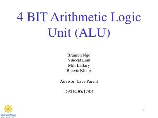
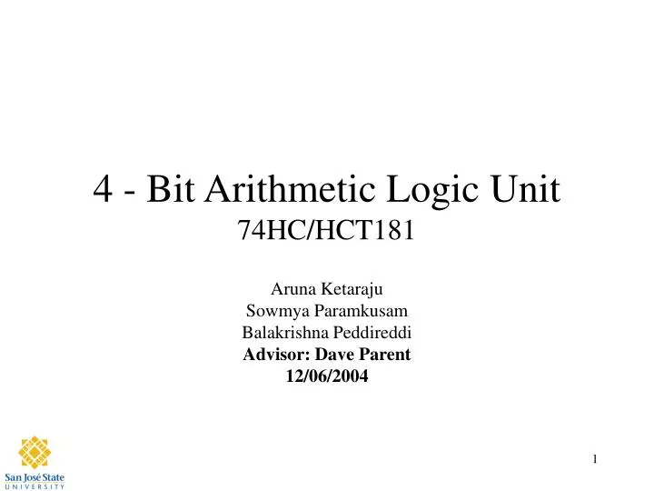
4 - Bit Arithmetic Logic Unit 74HC/HCT181. Aruna Ketaraju Sowmya Paramkusam Balakrishna Peddireddi Advisor: Dave Parent 12/06/2004. Agenda. Abstract Introduction Design Process Methodology Logic Verification Worst-case Delay Calculations Results Cost Analysis Conclusions. Abstract.

E N D
4 - Bit Arithmetic Logic Unit74HC/HCT181 Aruna Ketaraju Sowmya Paramkusam Balakrishna Peddireddi Advisor: Dave Parent 12/06/2004
Agenda • Abstract • Introduction • Design Process Methodology • Logic Verification • Worst-case Delay Calculations • Results • Cost Analysis • Conclusions
Abstract • We designed a 4-bit Arithmetic Logic Unit that operates at 200 MHz and uses 20.3W/cm2 of Power and occupies an area of 710x340mm2. • Full look-ahead for high speed operation on long words. • Arithmetic operating modes: -Addition, Subtraction • Logic function modes: - NAND, AND, OR, NOR, EX-OR, Comparator plus ten other logic operations.
Introduction • The 74HC/HCT181 is a 4-bit ALU. • Controlled by S0, S1, S2, S3, M. • For M = High , Logical operations are performed • For M = Low & Cn = High, Arithmetic operations are performed. • It can perform 16 arithmetic and 16 logical operations.
Design Process Methodology of the ALU • Sizing Transistors through the use of analytical equations. • Cell-based circuit implementation. • Simulation. • Layout. • Design Rule Check. • Layout versus Schematic Check. • Extraction. • Post Simulation
Logic Diagram Philips 74HC/HCT181
DFFs • DFFs are placed on either side of the combinational logic. • The DFF drives a load of 14.5fF and based on that the Wns and Wps are calculated. • The set-up and hold-times are .59ns and .63ns respectively.
Longest Path Calculations Note: All widths are in microns and capacitances in fF
Verification LVS REPORT
Worst-case Delay Calculations Longest Path is between B2 and A=B. The test vectors to calculate the worst-case propagation delay are: A0, A1, A2, A3, B0, B1, B3, S1 = 0; M, Cn = 1; B2 = toggle;
Cost Analysis Time spent on each phase of the project • Verifying logic : 3days • Verifying timing : 7days • Layout : 15days • Post extracted timing : 7days
Lessons Learned • Every PMOS should be in contact with n-tap. • Never route with poly. • The input data shouldn't near the clock rising edge.
Conclusions • 4-bit ALU has been simulated and verified • Frequency, area and power specifications have been met.
Acknowledgements • Thanks to Cadence Design Systems for the VLSI lab • Thanks to Synopsys for Software donation • Thanks to Prof. Parent for his support and guidance in each and every step of the project.