Download
1 / 26
270 likes | 286 Views
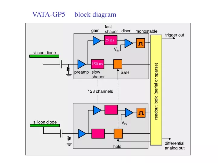
VATA-GP5 block diagram. fast. gain. discr. monostable. shaper. trigger out. 25 ns. V. thr. silicon diode. 150 ns. preamp. slow. S&H. shaper. 128 channels. readout logic (serial or sparse). silicon diode. V. thr. differential. hold. analog out.

E N D
VATA-GP5 block diagram fast gain discr. monostable shaper trigger out 25 ns V thr silicon diode 150 ns preamp slow S&H shaper 128 channels readout logic (serial or sparse) silicon diode V thr differential hold analog out
VATA-GP5 Principle of serial readout fast shaper discr. OR VFP FOR Trigger mask tresh. Det. S/H Analog Out slow shaper
VATA-GP5 Principle of sparse readout 1 FOR Register 128 1 0 1 0 Analog Out Channel address Look Up Table Data lock 7
Experimental set-up for VATA-GP5 tests with photoeelectrons VME DAQ Readout card CsI photctahode (300 nm) Deposited on a grid (Au, 80% transparency) Si sensor (300 mm) 208 pads (4×4 mm2) mask (at ground) photo- electrons -UPC = 15-20 kV UV H2 flash lamp (self triggering) vacuum pump (turbo) P < 10-5 mbar CaF2 MgF2 mirror MgF2 collimator
Vin versus Uth (Pulse Gen.) (fig. 9)
Discrimination Curve with lamp LSF: Q(fC) = 2.85 + 0.35 Uth (mV) Gain HPD = 4 * 103 – LSO crystal bars Eth ~ 15 Kev (fig. 14)
-1.45 + 150.8 * Vin -8.6 + 147.3 * Vin (fig. 7)
Si Sensor Depletion (Upc = 15 kV) (fig. 13)
Uth = 20 mV 1.56 fC / ADC count Pad # 205 Npe ~ 575 pad # 213 Npe ~ 285 (fig. 15)
2 2 1 1 Chip 1 Chip 2
2 1