Download
1 / 12
130 likes | 820 Views
Low power linear feedback shift register with clock gating. Course: Low power design of electronic circuits Student: Ahmed Faraz. Index. Objective Basic idea Basic gating circuit and linear feedback shift register Design platform Final circuit Results Conclusion. Objective.

E N D
Low power linear feedback shift register with clock gating Course: Low power design of electronic circuits Student: Ahmed Faraz
Index • Objective • Basic idea • Basic gating circuit and linear feedback shift register • Design platform • Final circuit • Results • Conclusion
Objective • To reduce the power of 16-bit linear feedback shift register(LFSR) using gated clock. • To measure the Average, Maximum and Minimum Power in Traditional 16-bit LFSR. • To measure the Average , Maximum and Minimum Power in 16-bit gated clock LFSR.
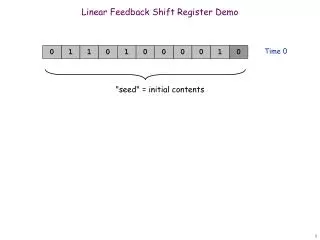
What is Linear feedback shift register? • A linear feedback shift register (LFSR) is a shift register whose input bit is a linear function of its previous state. For 16 bit LFSR-feedback polynomial is x16 + x14 + x13 + x11 + 1
Basic idea • Since, in LFSR, the clock-path of all flip-flop toggles at every clock cycle, they consume a significant amount of power. • To activate flip flop only when the input signal is different from the actual output value.
Conclusion • Average power consumed has been decreased, whereas Minimum power has been increased which may be due to the initial power consumption at the time of initializing the LFSR.
References • Dr. Vishwani Agrawal: Slides Spring 2009.Low Power Design of Electronic Circuits. • “Utilizing clock-gating efficiency to reduce power” • By Mitch Dale: EE TIMES-INDIA JANUARY 2008 • “Gated-Clock Design of Linear-Feedback Shift Registers” • By Walter Aloisi and Rosario Mita: IEEE TRANSACTIONS ON CIRCUITS AND SYSTEMS-2: EXPRESS BRIEFS, VOL.55,NO.6,JUNE 2008.