Download
1 / 21
1.87k likes | 4.18k Views
Printed Circuit Board Design. Sung Yeul Park Dept. of Electrical and Computer Eng University of Connecticut September 24, 2014. What can you see from an electrical engineering perspective?. Three Elements to be considered. Components : - How to select components?

E N D
Printed Circuit Board Design Sung Yeul Park Dept. of Electrical and Computer Eng University of Connecticut September 24, 2014
What can you see from an electrical engineering perspective? 2
Three Elements to be considered • Components : - How to select components? - What values are needed? - What kind of package will be? • Printed Circuit Board : - Schematic Design - PCB Layout Design - Prototype board • Case or Box for the prototype board : - Purchase or build by yourself 3
Printed Circuit Board ? A printed circuit board (PCB) mechanically supports and electrically connects electronic components using conductive tracks, pads and other features etched from copper sheets laminated onto a non-conductive substrate. PCBs can be single sided (one copper layer),double sided (two copper layers) or multi-layer. Conductors on different layers are connected with plated-through holes called vias. Advanced PCBs may contain components - capacitors, resistors or active devices - embedded in the substrate.
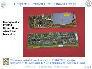
Printed Circuit Board Design A PCB as a design on a computer (left) and realized as a board assembly populated with components (right). The board is double sided, with through-hole plating, green solder resist and a white legend. Both surface mount and through-hole components have been used. 5
Printed Circuit Board Design Schematic Design 6 PCB Layout
Key terms for PCB design • Pads are where the components are soldered to the PCB. • Traces are the copper tracks that connect pads together. • Via are small holes through the board that link a bottom and top trace together electrically. Traces on the same layer cannot cross, so often, when you are laying out a PCB, you need to a signal to jump from one layer to another. 7
Key terms for PCB design • Silk-screen refers to any lettering that will appear on the final board. • Solder-mask is a layer of insulating lacquer that covers both sides of the board except where there are pads. 8
Multi-layer PCB design • 2 Layer PCB design: Top layer and bottom layer • 4 Layer PCB design: Top, Bottom, and two middle layers. 9
PCB design procedure • Design specification • Circuit diagram • Schematic design Select components Check the dimension Build a footprint Make a PCB library Add parts • Export schematic design to layout design • Route all connection • Design rule check • Generate Gerber files and drill file and zip them • Upload zip file to PCB order website 10
PCB Library design • Are you Ready to build a library? • Component datasheet • Dimension: mil (imperial unit) vs mm (metric) 1 inch =1000 mil, 1 mil = 0.0254 mm 1 mm = 39.3700787 mil DIP component and connector: 100 mil or 2.54 mm • Symbol in schematic vs Exact dimension in Layout • Pad number should be matched in schematic symbol and layout footprint 11
PCB Library dimension example • Male header 12
PCB manufacturing procedure http://www.pa-international.com/images/stories/Multi-layer%20Metal%20Plate%20PCB%20Process%20Flow%20Chart.JPG 13
Tips for PCB design • Keep traces straight, • Try to avoid 90o turns use two 45o’s. • Double, even triple check layout, • Having a fresh pair of eyes look it over, • “measure twice, cut once” idea. • Trace thickness & spacing • Spacing of at least .010”, • 0.030” for In-house • ~0.025” per 1 Amp carrying lines, • Don’t use anything smaller than 0.010” for traces, • 0.030” for In-house milling. • Try to keep all connections on one side of PCB • Take into account component package 14
Free PCB design program • EAGLE PCB Design Software: http://www.cadsoftusa.com/download-eagle/freeware/ • Express PCB: http://www.expresspcb.com/expresspcbhtm/download.htm • Free PCB: http://www.freepcb.com/ • Advanced Circuits: http://www.4pcb.com/free-pcb-layout-software/ 15
Making PCBs • Layout your circuit / circuits • Check out http://www.expressPCB.com for some great tips on component layout and power distribution. • Layout is more of an art. • Tight spaces • Lots of connections • Make a 2 level board into a 3 level with vias 16
DSP Board DC-AC Inverter DC-DC Converter 20
PCB Design Assignment • Every senior design team need to design one printed circuit board during fall semester. • The number of components should be more than 10 components with connectors, surface mount components, through-hole components, and ICs. • The number of layers should be 2 or more. • Report due date is November 19th 2014 • Report: Schematic, Layout, and Free dfm Check result • https://www.my4pcb.com/net35/FreeDFMNet/FreeDFMHome.aspx 21