Download
1 / 12
180 likes | 805 Views
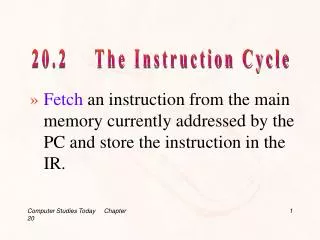
Instruction Cycle vs Clock Cycle. Instruction Cycle: The time required to fetch and execute an instruction Clock Cycle: one clock cycle, during which one step of an execution is completed.

E N D
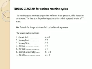
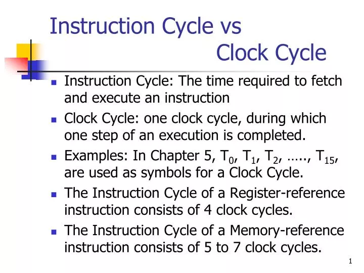
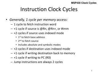
Instruction Cycle vs Clock Cycle • Instruction Cycle: The time required to fetch and execute an instruction • Clock Cycle: one clock cycle, during which one step of an execution is completed. • Examples: In Chapter 5, T0, T1, T2, ….., T15, are used as symbols for a Clock Cycle. • The Instruction Cycle of a Register-reference instruction consists of 4 clock cycles. • The Instruction Cycle of a Memory-reference instruction consists of 5 to 7 clock cycles.
Example: Adding two 32-bit numbers (A and B) by using the 16-bit Basic Computer • C = A + B • Split A into 16 bit numbers: AX: more significant 16 bits; AY: less significant 16 bits • Similarly B and C can be written as BX:BY and CX:CY respectively. • Store Carry-out from MSB in CZ.
Storing data in memory4K memory locations: 000 to FFF in HEX
Q1The Table shows, at T0, contents of one register, two flip-flops and some of the memory locations: Note: Use Figure 5-4 and Table 5-6 from your text-book for solving Q 1 and Q 2.
Q 1: Problem in Steps Step 1: The first memory instruction at address 445 is executed. While executing this instruction, during clock cycle T4, R is set to 1. Step 2: Three clock cycles of interrupt process are executed. At the end of this step R is cleared. Step 3: The second memory instruction at address 001 is executed.
Q 1: To Do ……….1 • Specify the register transfer operation(s) being executed during each clock cycle. • For Step 1, answer the following: • What is the value of I immediately after the clock cycle T2 is over? • Which instruction is being executed during this Step? • For Step 2, answer the following: • What is the value stored at address 0, immediately after clock cycle T1 is over? • What are the values of IEN and R immediately after the clock cycle T2 is over?
Q 1: To Do ……….2 • For Step 3, answer the following: • What is the value of I immediately after the clock cycle T2 is over? • Which instruction is being executed during this Step? • Specify the contents (in hexadecimal) of registers PC, AR, DR, AC, IR and TR at the end of each clock cycle. If the contents of a register are not yet known, specify it as X.
Q2The Table shows, at T0, contents of two registers, two flip-flops and some of the memory locations:
Q 2: Problem in Steps Starting with the above initial values at T0, the following steps are taken in sequence: • Step 1: First the memory instruction at address 2A2 is executed. • Step 2: After executing Step 1, the memory instruction at address 446 is executed. During execution of the two steps, for each clock cycle, starting from T0 for each of the steps, work out the following:
Q 2: To Do ……….1 • Specify the register transfer operation(s) being executed during the clock cycle. • For Step 1, answer the following: • What is the value of I immediately after the clock cycle T2 is over? • Which instruction is being executed during the Step? • For Step 2, answer the following: • What is the value of I immediately after the clock cycle T2 is over? • Which instruction is being executed during the Step? • What is the value of E immediately after the clock cycle T5 is over? • Specify the contents (in hexadecimal) of registers PC, AR, DR, AC and IR at the end of each clock cycle. If the contents of a register are not yet known, specify it as X.


![Tricarboxylic acid cycle (TCA Cycle) [Kreb’s cycle] [Citric acid cycle]](https://cdn3.slideserve.com/6696193/tricarboxylic-acid-cycle-tca-cycle-kreb-s-cycle-citric-acid-cycle-dt.jpg)