Download
1 / 30
300 likes | 468 Views
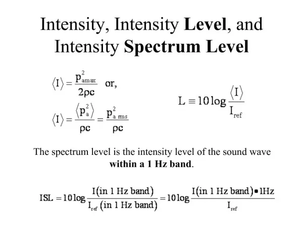
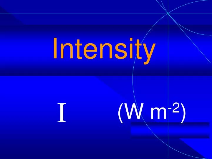
Intensity. I. (W m - 2 ). Intensity = Power. Area. P. I =. A. Inverse square law. I d 2 =. I d 2. A A. B B. Photoelectric effect. current. f o. frequency. Energy of photons. E = h f. h is Planck’s constant. Intensity of photons. I = N h f.

E N D
Intensity I (W m-2)
Intensity = Power Area P I = A
Inverse square law I d2= I d2 A A B B
Photoelectric effect current fo frequency
Energy of photons E = h f h is Planck’s constant
Intensity of photons I = N h f N is number of photons per second
Work function Minimum energy to release electron from a surface (E = h fo)
Kinetic Energy E = h f - h fo Energy above minimum appears as kinetic
Emission spectra W2 red W1 violet W0
Emission spectra W2 – W1 = h f Electron ‘jumps’ from excited level to lower level
Emission spectra Bright emission lines - more electrons
Absorption spectra W2 Photon ofenergyh f W1
Absorption spectra W2 = W1+ h f Electron absorbs radiation and ‘jumps’ to excited level
Spontaneous emission random process
Stimulated emission Photon (energy h f) can cause atom to emit photon (energy h f) in phase and same direction
Laser E1 Stimulating photon (hf) E0
Laser Monochromatic Coherent Intense
Semiconductors n-type p-type
n-type Conduction by negative electrons
p-type Conduction by ‘positive’ holes
Forward-biased n-type p-type electrons diode conducts
Reverse-biased n-type p-type diode does not conduct
Diode Forward-biased diode electron and hole recombine Photon (heat) emitted
LED Forward-biased diode electron and hole recombine Photon (light) emitted
photodiode Photovoltaic mode supplies power e.g. solar cell
photodiode Photoconductive mode (reverse bias) light sensor
MOSFET n-region implant drain oxide layer n-channel gate p-type substrate source n-channel enhancement MOSFET
MOSFET Can switch on a load. Apply gate voltage VGS to turn ‘on’ MOSFET
MOSFET + V load D Io G S VGS 0 V n-channel enhancement MOSFET
MOSFET Can also be used as an AMPLIFIER