Download
1 / 30
310 likes | 469 Views
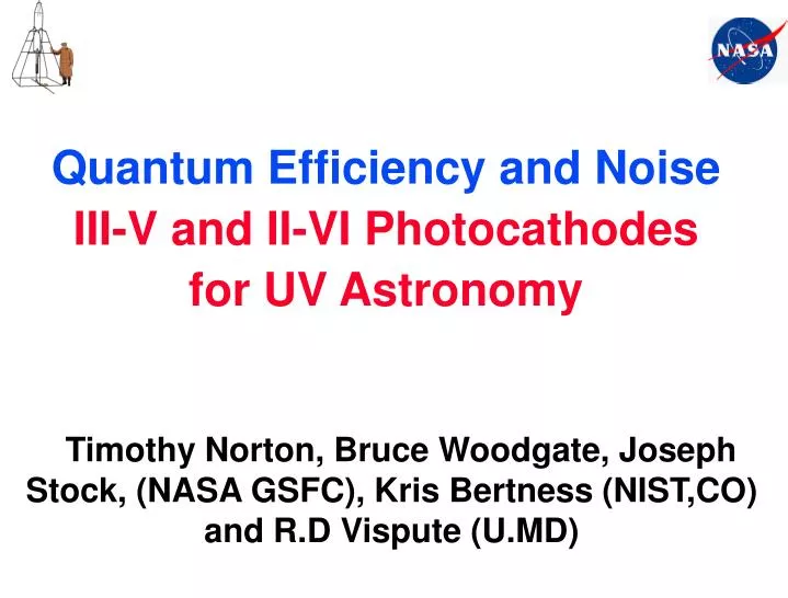
Quantum Efficiency and Noise III-V and II-VI Photocathodes for UV Astronomy . Timothy Norton, Bruce Woodgate, Joseph Stock, (NASA GSFC), Kris Bertness (NIST,CO) and R.D Vispute (U.MD). Overview. Our photocathode application in UV space-based astrophysics

E N D
QuantumEfficiency and NoiseIII-V and II-VI Photocathodesfor UV Astronomy Timothy Norton, Bruce Woodgate, Joseph Stock, (NASA GSFC), Kris Bertness (NIST,CO) and R.D Vispute (U.MD)
Overview • Our photocathode application in UV space-based astrophysics • Current NUV (100 - 320 nm) photocathodes and detectors - QE problem • Gallium nitride (and alloys) a high QE III-V photocathode • Our experience processing planar - opaque mode GaN and measuring GaN quantum efficiency • Summary of the status of ours and others GaN work • Nano-structuring GaN • Noise • ZnO a II-VI photocathode candidate • Conclusions
NUV photon-counting detector detector QE MCP based UV photon-counting detectors are the workhorses of UV astronomy. (EBCCD/CMOS detectors can also serve as useful UV photon counting detector readout) • They utilize a variety of photoemissive layers as the primary detection medium. • For space-based astronomy missions QE and noise are paramount factors • QE scales directly to required mirror size – payload size, weight and cost • High QE enables new science discovery reach
State of the art - Photocathode based UV photon-counting detectors HST-STIS/ACS/COS MAMA GALEX Delay line - UCB Excellent photon-counting detectors but they rely upon CsTe < 12% peak efficiency in the NUV. Their visible equivalents – CCDs – QE peak > 90 %
Gallium Nitride – a III-V photocathode • GaN – Direct Band Gap material, 3.2eV • Electron affinity 4.1 eV • Can be cesiated to NEA • Alloys – In for red response, Al for short wavelength cutoff • Substrate match to sapphire • Industry leverage – Blue LED – Bluray etc • Photocathode development - active Groups : NASA GSFC, UCB, NWU, SVT Associates, POC/TDI and Hamamatsu. After p-doping with Mg and cesiation - NEA
Spicer 3-step model • QE depends upon :- • 1) Absorption of photon - Reflection (angular dependence) • 2) Electron- transit to the Surface • Random walk • e--e- scattering, • phonon - trap scattering • Transit through depletion layer • 3) Escape surface probability • Overcome Work function • Reduction of due to Cs dipole or applied field (Schottky Effect)
Spicer 3-step diffusion model P – Escape probability – P-doping, Cs/CsO), surface cleanliness. R – Reflectivity - Morphology a – Absorption coeff – doping level. L – Diffusion length – (doping level,traps,quality) QE = P (1 - R(l)) a(l)L 1 + a(l) L For NEA cathodes : a(l) L >> 1 L > 1 micron
GaN sample mounting GaN suppliers :- SVT Associates NWU TDI/Oxford Instruments NIST, CO
25 nm SVT 0.1 micron GaN, planar. Vertical scale magnified.
P-Doping – Band bending and escape probability • Optimum acceptor (Mg) doping required for high QE. • Too low results in minimal band bending – low escape probability. • Too high increases minority carrier scattering and trapping. • We (GSFC have too limited data set to verify optimum level) • Hamamatsu Inc (Uchimaya) show 3 x 10^19 cm^-3) optimum level.
Basic GaN photocathode process • Acquire p-GaN – Vendors, SVT, TDI, NWU, NIST. • Cut into 1 cm squares – mount into sample holders. • Wet etch – Pirahna + HF, DI rinse – N2 bagging. • Button heater anneal > 2 hrs at 600C. • Electron scrub – 300 eV electrons, 1600 microamp/hrs. • Cesiation – SAES sources – 15 minute process – over cesiate. • Calibrate at 121, 150, 180, 254 nm vs CsTe – NST calibrated diode. • Decision to seal into device.
Surface preparation is crucial ! Piranha wet etch :- H2S04 + H202 (3:1) 10 min.- 90C; DI H20 rinse 5 min.; H2O + HF (10:1) 10 sec dip; DI H2O rinse 10 min.; Blow dry with N2. Package in clean, sealed N2-purged bag. Vacuum bake – UHV chamber – 350 C – 24 hrs Button heater - 600 C for 2 hrs Electron scrub – 300 eV electrons – 160 m/hr dose Cannot overstate importance of these process steps in improving QE.
Secondary effects • Electron mirror induced field due to higher band gap substrate heterostructure AlN/GaN – we see thinner GaN < 0.2 micron shows higher QE than > 1 micron thicker samples. • Piezio strain field in GaN due to substrate mismatch – not confirmed
GaN thermionic noise • The noise of a wide band gap emitter without high internal fields (eg. a TE photocathode) such as GaN will be dominated by the electron diffusion current in the bulk absorber region multiplied by the thermalized electron escape probability. • We are setting up a MCP based system to measure • UCB – already measured few counts/cm/s.
Quantum efficiency stability Sealed tube – GaN quantum efficiency lifetime Can be assumed long term quiescent stability demonstrated
Nanowire structuring • Nanowires may lead to higher QE due to :- • Higher absorption – analogous to “Black Silicon” • Much higher crystal purity – longer diffusion length and QE • Can match a variety of layers eg Silicon MCP substrates.
GaN matrix layer Si (111) substrate ~ 1 m <1100> Si <110> GaN nanowire (p-doped) at NIST, CO <0001> GaN nanowires AlN buffer 50-80 nm Grown at 635 °C 200 nm Al prelayer 0.5 nm No catalyst Wire growth in range 810 to 830 °C MBE with plasma-assisted N2 source Low Ga flux and high nitrogen flux Smaller wires have perfect hexagonal cross-section, aligned to substrate and therefore to each other Both wire tips and matrix are Ga-face as determined by CBED and etching
NIST, CO GaN Nanowires Recent sample shows un-cesiated QE > 30 % at 121nm
Detectors with GaN processed and sealed at GSFC Diode tube EBCCD tube – Photek resealed by GSFC
ZnO • Potential advantages – much lower intrinsic defect levels than GaN, can be matched to a large variety of substrates, can be readily grown in nanowire configurations. • Problems – intrinsically n-type difficulty in p-doping,– same solubility issues as GaN • Phosphorous p-doping has recently been demonstrated by UMD.
University of Maryland ZnO research Wide band gap thin film Zn(1-x) MgxO system is capable of tuning a band gap from 3.3 eV to 7.9 eV for visible blind UV detection. Selective area growth of nanowires can be facilitated using diamond-like carbon film as a pattern and nucleation layer.
Conclusions • State of the art III-V opaque mode photocathodes eg GaN can attain very high QE in the NUV > 72 %, (as demonstrated by GSFC,UCB,Hamamatsu). • p-Doping level is crucial in optimizing yield. • Surface preparation also very important. • Alloying with In or Al can extend wavelength response. • Nanowire structuring may yield higher QE via improved diffusion length and reduced reflectivity and optimized absorption. • Main challenge - matching to usable detector substrates including Silicon and Ceramic MCPS to be demonstrated.