Download
1 / 17
190 likes | 563 Views
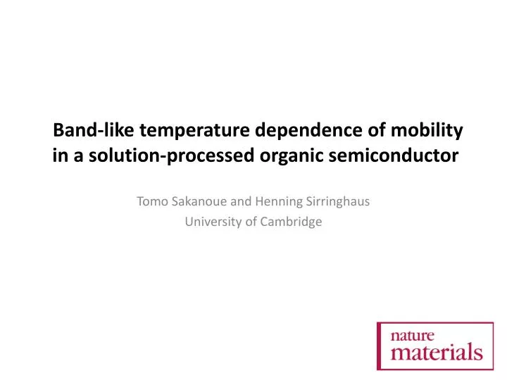
Band-like temperature dependence of mobility in a solution-processed organic semiconductor. Tomo Sakanoue and Henning Sirringhaus University of Cambridge. What is the nature of charge carriers and transport in OSCs?.

E N D
Band-like temperature dependence of mobility in a solution-processed organic semiconductor TomoSakanoue and Henning Sirringhaus University of Cambridge
What is the nature of charge carriers and transport in OSCs? • In inorganic semiconductors charge carrier transport occurs via band-like transport. In organic semiconductors transport is not well understood. • Authors suggest that band-like transport does not occur in organics at room temperature and that the charge carriers are localized. • Polaron (charge and deformation of conjugated chain) – self trapped by the deformation • Molecular vibrations can also destroy translational symmetry between neighboring molecules – causing a mismatch in HOMO or LUMO alignment causing charge trapping • Typically mobility temperature dependence in semicrystalline and polymeric films has indicated the hopping mechanism, however increased mobility has been seen for very pure crystalline small molecule films (rubrene) indicating band-like transport. • Band-like transport is limited by scattering of the carriers (electrons or holes) on phonons (thermally induced crystal lattice deformations). Therefore an indication of band-like transport is increased mobility at low temperatures.
p – Channel FET • Enhancement mode: a small gate voltage enhances the source – drain current • Majority carriers (holes) flow from source to drain therefore in a p-channel FET drain potential must be lower than source. • As a reverse bias is applied at the gate, the negative potential induces a positive substrate channel immediately below the gate, and the hole current increases as the reverse bias at the gate increases.
Device Architecture P-channel field effect transistor, top gate, bottom contact architecture low dielectric constant polymer used to insolate the gate electrode Gate Insulator Channel Source / Drain Polyimide layer inserted to control wettability of glass substrate PFBT (Pentafluorobenzenethiol) / Au Polycrystalline organic semiconductor, domain size over 100 mm.
p – Channel FET, Room Temperature Properties • Output characteristics of a device with relatively short channel length L = 5 mm, channel width W = 100 mm and a 120-nm-thick dielectric • Majority carriers (holes) flow from source to drain therefore in a p-channel FET drain potential must be lower than source(so negative drain potential applied) • As a reverse bias is applied at the gate, the negative potential induces a positive substrate channel immediately below the gate, and the hole current increases as the reverse bias at the gate increases. Current increases with drain voltage until maximum output is reached (saturation region). • Second graph displays gain (amplification, ratio of output signal to input) of current due to gate voltage.
Temperature Dependence • For intermediate drain and gate voltages (-15V), the FET current was nearly temp independent between rt and 200 K, but then decreased with decreasing T. • For higher voltages (VD, G = -30 V) Current increases by ~25% on cooling from r.t. to 140 K; even at 4.3 K current remains same as r.t. • Room temp to 140 K, the output I-V curves have clear linear and saturation regions. However, below 140K they acquire a positive curvature. • The increase in transistor current between rt and 140K demonstrates unambiguously that, in contrast to other organic FETs, charge transport in TIPS-pentacene FETs at sufficiently high applied voltages improves with decreasing temperature. Temp dependence of ID as function of VD, VG = -30 V
Field-effect Mobility Square root of drain current as a function of gate voltage, with drain voltages of VD = -15 and -30 V. Temperature dependence of the effective mobility of TIPS-pentacene FETs with different VD. Ci = Capacitance of gate dielectric VG = Gate Voltage, VT = gate voltage at which channel conductance can begins • Mobility can be extracted from the slope of the square root of the drain current in the saturation regime. • Mobility in low voltage devices (VG,D = -15V), increases from 300K to 200 K but then decreases below 200 K. Mobility is effected by trap states (energetic disorder pentacene/Cytop interface); at higher temperatures the more mobile states higher in the density of states have been populated thermally and mobility increases with decreasing temperature. • Where high gate voltages are used (trap states are filled) the mobility in these more mobile states can be estimated. Can see mobility increases with decreases temperature (down to 140 K) , reaching value of 2.5 cm2V-1s-1
Charge Modulation Spectroscopy • Localized, polaronic charges in organic semiconductors have characteristic optical absorptions differing from the neutral p-p* absorption, such as the transitions between that HOMO and SOMO and SOMO and LUMO of the radical cation. • CMS modulates the charge density in the semiconducting film by modulating the applied ac gate voltage . By measuring the DT, the characteristic spectroscopic signature of the field-induced charge can be detected. • Neutral TIPS-Pentacene (2.0 eV) and radical cation (formed using FeCl3) • Radical cation: 0.94-1.48 eV and 2.8 eV (0.94 eV possibly SOMO-LUMO and 1.32-1.48 eV HOMO-SOMO)
Charge Modulation Spectroscopy • At low temperatures the spectral shape becomes very similar to that of the isolated radical cation in solution. • Resemblance to the absorption of the radical cation in solution, the charges are not fully extended but remain localized over a certain N number of molecules. • CMS spectra in combination with T dependent mobility indicates charge carriers in device are localized not by polaronself-localization, but dynamic lattice disorder: small room temperature molecular motions that are sufficient to destroy the translational symmetry of the electronic Hamiltonian (representing a stack of molecules). – offsetting neighboring HOMO and LUMOs from each other. • T dependent CMS of FETs • (L = 40 mm, 450 nm thick dielectric, zero lateral electric field) • Blue absorption of TIPS-pentacene thin film on polyimide coated glass substrate. CMS at 43 K (black) and difference between the absorption spectra of a chemically doped and undoped solution (red)
Conclusions • At low drain and gate voltages trap states in TIPS-pentacene thin films inhibit mobility but at high drain and gate voltages trap states are filled and more mobile states can be accessed. • In TIPS-pentacene polycrystalline p-channel FETs charge carriers show spectroscopic signature similar to radical cation, but also a temperature dependent mobility where m increases at T decreases. • The charge mobility is therefore not band-like as in inorganic semiconductors, but also not polaron trapped as in some polymer thin films. The charge carriers are localized, but experience an increased mobility at low temperature due to freezing of intermolecular motions.
Charge Modulation Spectroscopy • The origin of the nonlinear dependence of the low-temperature transport on the lateral electric field. • Keeping lateral field constant (constant VD) carried out low temp CMS. • The sharp peak at 1.24 eV (trapped-charge absorption) broadens with increasing VD. • Spectrum at 100K and -15 V is very similar to the broad charge-induced at 300K, VD = 0. • This provides evidence that charges in single-molecule, shallow trap states can be effectively detrapped into more mobile states by application of the source-drain electric field. Drain-voltage dependence of the CMS spectra at 100 K. For comparison, the corresponding spectrum at 300K and VD= 0 V is also shown. All spectra were acquired with VG = -20 V and a modulation bias of ±2 V at 37 Hz.
What is the nature of charge carriers and the mechanism of charge transport in organic semiconductors (OSCs) at room temperature? Band-like Transport In comparison to covalently bonded inorganic semiconductors, OSCs are characterized by weak intermolecular van der Waals bonds; this leads to relatively narrow bandwidths, stronger electron lattice interactions, and more pronounced polaron formation. Consequently, coherent band-like conduction is expected only at low temperatures. As temperature increases, electron-phonon coupling leads to enhancement of polaron mass and further decrease in bandwidth, this may ultimately result in localizing charge carriers and altering the transport mechanism. Therefore band-like m should improve with decreasing T. Highly pure single crystals of small molecule OSCs (i.e. rubrene)electronic conduction improves with decreasing temperature: charge carriers occupy states that extend over many molecules Hopping If transport is occuring via phonon assisted hopping mwill decrease with decreasing T. In contrast electronic conduction in many polymeric or polycrystalline OSCs degrades exponentially with decreasing T.
Field-effect Mobility Square root of drain current as a function of gate voltage, with drain voltages of VD = -15 and -30 V. Temperature dependence of the effective mobility of TIPS-pentacene FETs with different VD. • Mobility can be extracted from the slope of the square root of the drain current in the saturation regime. • Sq. root of the saturated drain current exhibits a positive curvature at low gate voltages and the threshold voltage shifts to more negative values. This reflects filling up low-mobility trap states and eventually populating more mobile states. Where high gate voltages are used, the mobility in these more mobile states can be estimated. W = channel width, Ci= capacitance of the gate dielectric, VT = threshold voltage. q = absolute electron charge, fB= difference between the Fermi level and the intrinsic Fermi level (which is located very close to midgap), ei= permittivity of the gate dielectric.
Field-effect Mobility Square root of drain current as a function of gate voltage, with drain voltages of VD = -15 and -30 V. Temperature dependence of the effective mobility of TIPS-pentacene FETs with different VD. m (0) = mobility with zero applied field q = absolute electron charge F = magnitude of electric field Poole-Frenkel factor, b =(e/pee0) 1/2 m (F) = field-effect mobility k = Boltzmann constant • Mobility can be extracted from the slope of the square root of the drain current in the saturation regime. • Mobility in low voltage devices (VG,D = -15V), increases from 300K to 200 K but then decreases below 200 K. Mobility is effected by trap states (energetic disorder pentacene/Cytop interface); at higher temperatures the more mobile states higher in the density of states have been populated thermally and mobility increases with decreasing temperature. • Where high gate voltages are used (trap states are filled) the mobility in these more mobile states can be estimated. Can see mobility increases with decreases temperature (down to 140 K) , reaching value of 2.5 cm2V-1s-1