NBTI-Aware Synthesis of Digital Circuits
380 likes | 1.25k Views
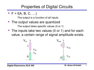
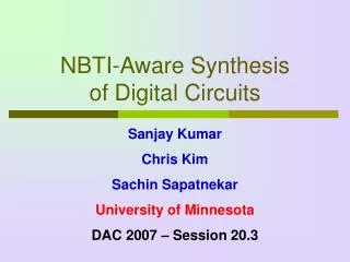
NBTI-Aware Synthesis of Digital Circuits Sanjay Kumar Chris Kim Sachin Sapatnekar University of Minnesota DAC 2007 – Session 20.3 -V dd 0 Si Si Si H H H 0 V dd V G = 0 V S = V dd V D G Oxide Poly Substrate D S oxide B H 2 SiH + h + → Si + + ½ H 2 V B

NBTI-Aware Synthesis of Digital Circuits
E N D
Presentation Transcript
NBTI-Aware Synthesis of Digital Circuits Sanjay Kumar Chris Kim Sachin Sapatnekar University of Minnesota DAC 2007 – Session 20.3
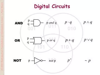
-Vdd 0 Si Si Si H H H 0 Vdd VG = 0 VS = Vdd VD G Oxide Poly Substrate D S oxide B H2 SiH + h+→ Si+ + ½H2 VB Negative Bias Temperature Instability (NBTI) Vdd Relaxation Stress S G VG = Vdd VG = 0 Increase in PMOS Vth gradually over a few years
Outline of this talk • Problem Description • How does NBTI affect circuits? • Modeling and Estimation • What parameters does it depend on? • Design for Reliability • How can we overcome this effect? • Results and Summary • How does our work compare with other solutions?
Problem Statement NBTI in PMOS devices Aging - circuits become slower Operate circuits at lower speeds NBTI-aware robust circuit design Design NBTI-resilient circuits with the least amount of overhead
Sizing for Reliability [DATE06, ICCD06, ISQED07] After 10 years Original design Gates become weak, target freq not met Area overhead Reliable design After 10 years Design sized accounting for aging Still meets specs
Worst case NBTI All PMOS devices degrade maximally Easy to estimate impact Conservative and pessimistic Actual Circuit Operation NBTI effect based on Signal Probability (SP) Each node has a certain SP Worst case can never happen 1 1 0.25 0.5 1 0.5 1 0.25 1 0.375 1 0.5 1 0.5 1 0.375 1 0.5 “Worst Case” NBTI Assumption
Limitations of Sizing based flow Sizing 10 years aging Nominal Timing Spec = T0 ps. New Timing Spec = 0.91T0 ps. 10% delay increase Allows changes in gate sizes only Synthesize circuits accounting for NBTI-induced delay degradation.
Focus Incorporate NBTI-guard banding into synthesis during tech-mapping Reduce pessimism in estimation of aging effects Design best NBTI tolerant structures Requirements NBTI-aware library characterization Signal probability of primary inputs Suitable cost function (delay, area, power, etc) in tech-mapping Our Work
NBTI Modeling and Library Characterization Key Results
Vdd NBTI Model (ICCAD06) • NIT strong function of Signal Probability (SP) • Electrical parameter: ΔVth NIT Vdd 0 PMOS under Stress Interface trap generation NIT increases as t(1/6) PMOS under Relaxation Annealing of existing traps NIT decreases
Vdd Vth Degradation Vdd 0 Vthmax Signal Probability: Probability that the signal is low
A Inverter Characterization Build a model of delay versus signal probability
Path from B A B Path from A A B NAND Gates
1 0.66 0.33 SP of A 0 SP of B NOR Gates – PMOS Stacking B A B A
Technology Mapping SiS – synthesis tool 42 gates (NOT, NAND2, NAND3, NOR2, NOR3, AOI12, AOI22, OAI12, OAI22)
Nominal Synthesis Library: Delay of gates characterized assuming no NBTI (Nominal PMOS Vth) Logic cone: Boolean function realized at each node Cost function: Minimum area that meets the target delay Compute delay of different candidate blocks at each node Choose the structure with the best cost function
NBTI-Aware SP-based Synthesis Library : Delay of gates characterized for each signal probability Library: Delay of gates characterized assuming no NBTI (Nominal PMOS Vth) Logic cone: Boolean function realized at each node Cost function: Minimum area that meets the target delay Logic cone: Signal probability propagated from PIs to all nodes in subject graph Compute delay of different candidate blocks at each node Choose the structure with the best cost function Pick best candidate gate under a new metric for delay
0.6 0.4 0.3 0.7 0.3 0.5 0.5 0.574 0.4 0.6 0.4 0.426 0.18 0.82 0.18 0.7 0.3 0.7 Subject Graph NAND-NOT Dual Representation of the Subject Graph
0.6 0.4 0.4 0.3 0.7 0.18 0.82 0.5 0.5 0.82 0.7 0.3 0.4 0.6 0.574 0.426 0.426 0.6 0.5 0.7 0.18 0.7 0.3 Performing SP-based Synthesis
0.6 0.4 0.6 0.4 0.3 0.7 0.3 0.3 0.5 0.5 0.5 0.5 0.574 0.574 0.4 0.6 0.4 0.426 0.4 0.426 0.18 0.82 0.18 0.18 0.7 0.3 0.7 0.7 Performing SP-based Synthesis
0.4 0.6 0.6 0.3 0.7 0.5 0.5 0.5 0.574 0.426 0.6 0.426 0.4 0.4 0.82 0.18 0.7 0.7 0.3 Performing SP-based Synthesis Pushing nodes with large SP inside the gates
Worst Case Synthesis Pick best candidate gate under “worst case” NBTI-induced delay Library: Delay of gates computed using Vthmax for PMOS transistors Logic cone: SP of each node in subject graph set to 1 Cost function: Minimum area that meets the target delay Choose the structure with the best cost function Compute delay of different candidate blocks at each node
C17 - Synthesis Results Increasing size Tspec = 70ps Circuit fails with aging Nominal synthesis Area = 7.4µm Worst case synthesis Area = 11.6µm SP-based synthesis Area = 9.8µm
Nominal Timing Spec SP based 10 years Worst case Temporal Degradation of Circuits Data for Benchmark C432
Summary • NBTI (aging) in circuits causes delay degradation • Need to relax timing or design NBTI-resilient circuits • Area increase to counter effect of Vth degradation • NBTI-aware optimal synthesis method presented • Signal probability based design reduces pessimism, leads to area savings over “worst case” methods
Thank You Questions and Comments
X1 X1 X2 X2 Synthesis versus Sizing Which one is better? Spec Delay Area Target lifetime (log scale) Time of operation (log scale)
What if…… • Signal Probability (SP) of primary inputs not equal to 0.5 • SP values closer to the “worst case” • Gain over “worst case” depends on library gates, sizes and SP distribution • Still better than sizing approaches • Can we set SP such that gain is maximized?
Worst case synthesis Area = 11.6µm 0.5 SP-based synthesis Area = 9.8µm C17 – Synthesis with Different SP Increasing size Tspec = 70ps 0.8 SP-based synthesis Area = 10.8µm
Vdd Vdd m k-m k = m * SP k Converting Random Waveforms to Deterministic Periodic Signals (SP, AF) Interface trap count for both these waveforms are equal “asymptotically”
Frequency Independence Vdd freq = f1 T1 n1 cycles Vdd freq = f2 n2 cycles T2 Number of interface traps for both cases same Trap generation independent of frequency
“sk” Notation – Multi-cycle Model Vdd q-p p p/q = SP q 0 < i ≤ p NIT(kt0) = sk NIT(t0) sk=nq+i = p < i ≤ q