Download
1 / 28
280 likes | 555 Views
Inelastic X-ray Scattering in Semiconductors. Jorge Serrano Institució Catalana de Recerca i Estudis Avançats Universitat Polit ècnica de Catalunya. Outlook. Inelastic X-ray Scattering: Fundamentals Applications in semiconductors: Single crystals: GaN , h-BN Thin Films: InN

E N D
Inelastic X-ray Scattering in Semiconductors Jorge Serrano InstitucióCatalana de RecercaiEstudisAvançats UniversitatPolitècnica de Catalunya
Outlook • Inelastic X-ray Scattering: Fundamentals • Applications in semiconductors: • Single crystals: GaN, h-BN • Thin Films: InN • Conclusions 18/08/2010 Universidad Autónoma de Querétaro
Information derived from IXS/INS data • Sound velocities • Elasticity • Interatomic force constants (potential) • Relaxation times • Dynamical instabilities (phonon softening) • Anharmonicity • Electron-phonon coupling • Thermodynamics (CV, SV, qD, …) 18/08/2010 Universidad Autónoma de Querétaro
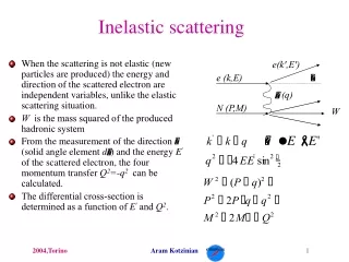
Counts per 2 minutes X-rays and phonon studies ? “When a crystal is irradiated with X-rays, the processes of photoelectric absorption and fluorescence are no doubt accompanied by absorption and emission of phonons. The energy changes involved are however so large compared with phonon energies that information about the phonon spectrum of the crystal cannot be obtained in this way.” W. Cochran in Dynamics of atoms in crystals, (1973) “…In general the resolution of such minute photon frequency is so difficult that one can only measure the total scattered radiation of all frequencies, … As a result of these considerations x-ray scattering is a far less powerful probe of the phonon spectrum than neutron scattering. ” Ashcroft and Mermin in Solid State Physics, (1975) DE meV !!! Einc > 10 keV !!! Photon flux ??? 18/08/2010 Universidad Autónoma de Querétaro
High resolution IXS: applications New materials GaN Geophysics Surfaces High Pressure Glasses & liquids 18/08/2010 Universidad Autónoma de Querétaro
Q = (4 p/l) sin(q) l1tunable sample l= 2d(T) sin qB detector E i E f l2 constant How does it work? • Backscatteringconfiguration • Specialanalyzers • Energyscans = temperaturescans • 0.25 mKtemperature control 18/08/2010 Universidad Autónoma de Querétaro
ID28 Layout 18/08/2010 Universidad Autónoma de Querétaro
kf, wf Q=q + G q // G : longitudinal mode q G : transverse mode ki, wi q kf Q q Wavevector k Energy E = ħck G Q ki q G S(Q,w) Q G determines the Brillouin zone q determines the physics IXS: The technique Q = ki - kf w = wi - wf 18/08/2010 Universidad Autónoma de Querétaro
WurtziteGaN T. Ruf, J. Serrano, M. Cardona, P. Pavone, M. Pabst, M. Krisch, M. D’Astuto, T. Suski, Grzegory, and M. Leszczynski, Phys. Rev. Lett. 86, 906 (2001) • Hexagonal structure (2H) • ABAB… • 4 atoms/unitcell12 branches in phonondispersionrelations • Commonstructuretomanyrelevantsemiconductors: ZnS, CdS, CdSe, ZnO, AlN, InN 1 cm 18/08/2010 Universidad Autónoma de Querétaro
WurtziteGaN T. Ruf, J. Serrano, M. Cardona, P. Pavone, M. Pabst, M. Krisch, M. D’Astuto, T. Suski, Grzegory, and M. Leszczynski, Phys. Rev. Lett. 86, 906 (2001) GaN 1 cm 18/08/2010 Universidad Autónoma de Querétaro
WurtziteGaN T. Ruf, J. Serrano, M. Cardona, P. Pavone, M. Pabst, M. Krisch, M. D’Astuto, T. Suski, Grzegory, and M. Leszczynski, Phys. Rev. Lett. 86, 906 (2001) • 3meV & 5.5 meVresolutionforacoustic and opticmodes • 1 week of beam time @ ID28 (ESRF) • Verylowstatisticsforopticmodes • 5h/day of sleep… GaN 1 cm 18/08/2010 Universidad Autónoma de Querétaro
WurtziteGaN T. Ruf, J. Serrano, M. Cardona, P. Pavone, M. Pabst, M. Krisch, M. D’Astuto, T. Suski, Grzegory, and M. Leszczynski, Phys. Rev. Lett. 86, 906 (2001) 18/08/2010 Universidad Autónoma de Querétaro
WurtziteGaN 18/08/2010 Universidad Autónoma de Querétaro
G. Kern et al., PRB 59 8551 (1999) h-BN: phonon dispersion relations • Small sample sizes: ~ 500 mm • Large neutron absorption cross section of 10B isotope • 30x60 mm2 beam : single domains available Bulk h-BN HR-EELS hBN/Ni(111) E. Rokutaet al., PRL 79 4609 (1997) 18/08/2010 Universidad Autónoma de Querétaro
60s Elasticity A. Bosak, J. Serrano, M. Krisch, K. Watanabe, T. Taniguchi, H. Kanda, Phys. Rev. B 73 041402(R) (2006) Institut de Ciència de Materials de Barcelona
60s A. Bosak, J. Serrano, M. Krisch, K. Watanabe, T. Taniguchi, H. Kanda, Phys. Rev. B 73 041402(R) (2006) J. Serrano et al., PRL 98 095503 (2007) IXS spectra 18/08/2010 Universidad Autónoma de Querétaro
Phonon Dispersion Relations J. Serrano, A. Bosak, R. Arenal, M. Krisch, K. Watanabe, T. Taniguchi, H. Kanda, A. Rubio, and L. Wirtz, Phys. Rev. Lett. 98, 095503 (2007) 18/08/2010 Universidad Autónoma de Querétaro
Phonon Dispersion Relations J. Serrano, A. Bosak, R. Arenal, M. Krisch, K. Watanabe, T. Taniguchi, H. Kanda, A. Rubio, and L. Wirtz, Phys. Rev. Lett. 98, 095503 (2007) 18/08/2010 Universidad Autónoma de Querétaro
HREELS vs. Ab initio calculations Bulk h-BN h-BN/Ni(111) Bulk h-BN h-BN/Ni(111) 18/08/2010 Universidad Autónoma de Querétaro
Grazing incidence IXS in InN J. Serrano, A. Bosak, M. Krisch, A.H. Romero, F.J. Manjon, N. Garro, M. Kuball, in preparation (2010) •Wurtzite & Zincblende structure WZ: a=3.54 Å, c=5.71 Å •Low band gap direct semiconductor (0.8 eV) •Applications in optoelectronics combined with other III-V nitrides • Grown as a thin film by epitaxy 6.2µm InN on GaN(0.5µm)/sapphire 18/08/2010 Universidad Autónoma de Querétaro
Grazing incidence scattering a = 3.5340 Å c = 5.7088 Å ρ = 6.93 g/cm3 InN @ 17.794keV αi = 0.12° Energy resolution: 3 meV 18/08/2010 Universidad Autónoma de Querétaro
WurtziteInN 18/08/2010 Universidad Autónoma de Querétaro
WurtziteInN J. Serrano, A. Bosak, M. Krisch, A.H. Romero, F.J. Manjon, N. Garro, M. Kuball, in preparation (2010) 18/08/2010 Universidad Autónoma de Querétaro
Conclusions • IXS: a maturetechnique, complementaryto INS, especiallyusefulfordetermination of phonondispersions in new materials, surfaces, and at highpressure. • Need of theoreticalsimulations in ordertoincreasethe data collection and success of theexperiment. • Semiconductors: thin films & surfacemodes • Otherapplicationsnotdiscussed: chargedensitywaves, superconductors, amorphousmaterials… 18/08/2010 Universidad Autónoma de Querétaro
Acknowledgements • ESRF: M.Krisch, A.Bosak, M. D’Astuto (U. Paris XI) • CINVESTAV: A.H. Romero • MPI-FKF: M. Cardona, T. Ruf (Bosch A.G.) • U. Valencia: N. Garro, A. Cantarero • DIPC: A.Rubio • CNRS (Lille): L.Wirtz • CEA (Paris): R. Arenal Samples: • UNIPRESS: T. Suski, I. Grzegory, M. Leszczynski • NIMS: K.Watanabe, T. Taniguchi, H. Kanda • U. Bristol: M. Kuball 18/08/2010 Universidad Autónoma de Querétaro