Download
1 / 23
230 likes | 503 Views
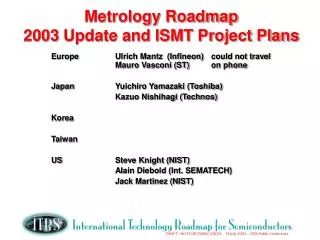
Metrology Roadmap. Alain Diebold. Metrology Roadmap 12-06. Europe Japan Masahiko Ikeno (Hitachi High-Technologies) Korea Soobok Chin (Samsung) Taiwan Jack Chung (Macronix) J.H. Sheih (TSMC) North America Steve Knight (NIST) Alain Diebold (SEMATECH).

E N D
Metrology Roadmap Alain Diebold
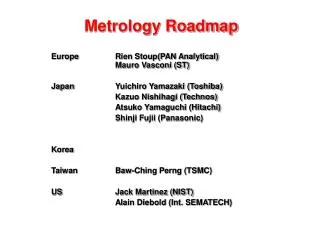
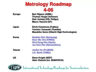
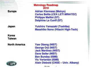
Metrology Roadmap12-06 Europe Japan Masahiko Ikeno (Hitachi High-Technologies) Korea Soobok Chin (Samsung) Taiwan Jack Chung (Macronix) J.H. Sheih (TSMC) North America Steve Knight (NIST) Alain Diebold (SEMATECH)
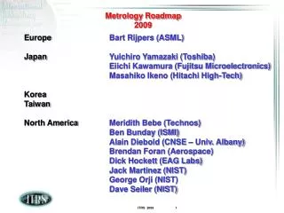
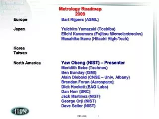
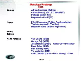
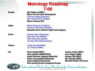
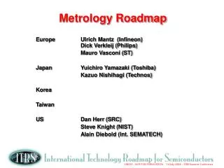
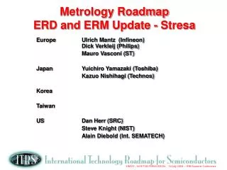
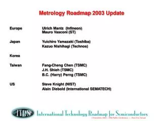
Metrology Roadmap7-06 Europe Bart Rijpers (ASML) Marco van der Haar (Panalytical) Thomas Hingst (Infineon) Dick Verkleij (FEI- Philips) Mauro Vasconi (ST) Japan Eiichi Kawamura (Fujitsu) Yuichiro Yamazaki (Toshiba) Masahiko Ikeno (Hitachi High-Technologies) Korea Soobok Chin (Samsung) Hyun Mo Cho (KRISS) Chul Hong Kim (Hynix) Jae Sam Kim (Nanometrics) Taiwan Jia-Rui Hu (ProMOS) J.H. Sheih (TSMC) US Steve Knight (NIST) Andras Vladar (NIST) Alain Diebold (SEMATECH) John Allgair (ISMI) Ingrid Peterson (Applied Materials) George Orji (NIST) Susie Wang (Applied Materials) Ben Bunday (ISMI) Andy Hegedus (Exponent) Meredith Beebe (Technos) Dick Hockett (Evans Analytical Group)
2006 New Areas • As Clean Rooms move to FOUPs and relax particle class do we need to spec humidity and temperature control ranges across fab?? Can we develop a correction algorithm instead? • Will a new method be needed for CD beyond the 32 nm Generation? • Can CD-SEM meet 32 nm dense line with matching • In-line TEM Sampling and cross-sectional metrology by Dual column FIB • Total Measurement Uncertainty vs Total Measurement Reproducibility • Calibration of ellipsometers and reflectometers at 193 nm
2006 New Areas • Local strain measurement in the channel • 3D Dopant Profiling for USJ: New requirements such as new structures (MUGFETs) and new processes (dopant anneals) • High aspect ratio measurements for Memory chips • 3D structure measurements (profile, roughness) • Total Measurement Uncertainty vs Total Measurement Reproducibility • Calibration of ellipsometers and reflectometers at 193 nm • Metrology for SiGe, Ge, and III-V Channels for transistors – epi layer quality • TEM and HR-XRD – more automated and TEM Tomography
2006 Activities • Dick Verkliej – add dual column FIB to Materials & Cont. Char section • Bart Rijpers – work on Litho Metrology section for TMU vs TTR & check CD precision coloring for tool matching • Thomas Hingst – draft standard terms for In-Line/Off-Line/In-Situ • STRJ-WG11 to send New Requirements lines for Stress/Dopant Profile • Everyone to obtain access to the ITRS Web site • Steve Knight & Thomas Hingst – define standard for references for n an k calibrations at 193 nm for lithography modeling • Ikeno-san - report in LER/LWR measurement definition from SEMI Micropatterning Committee Task Force
CD capability for single tool met(?) by single tool to 32 nm for Dense lines • Overlay P/T moves to 20% in 2007 • Double Patterning & Double Exposure drive tighter mask Metrology – update in 2007 Metrology Roadmap • Box in Box Overlay structures too large and will be design ruled out soon – Litho asks if overlay metrology will meet requirements associated with smaller targets? • EUV Reticle flatness at 32 nm ½ pitch needs to be measured on electrostatic chuck. Mask must be flat to within 32nm peak to valley 2006/2007 Changes to Litho Metrology
Dual patterning (two exposures with etch steps) overlay control Etch 2 Exposure 2 Etch 2 Exposure 1 Etch1 Resist BARC CD Litho 2 = Litho1 • Equal lines Overlay error • Different line width alternating Litho 2 > Litho1 • Thinner lines • Pairs of lines (AB:AB) • Across area CD’s identical
Resolution = DRAM ½ pitch node Resolution/3 Resolution/5 Resolution/15 Overlay RequirementsAs a function of Technology Node Double Patterning
LER/LWR Activities • Standard for LER and LWR will be Published in March 2007 by SEMI. • Defines measurement sampling length of 2 microns and sampling frequency of 10 nm or less. • Litho TWG and Metrology TWG need to now use new definition in requirements table in 2007!!
FEP Metrology:Expanded Emphasis on Areas beyond High k • Increase in Mobility by using local stressing of transistors – FEPCall for local stress metrology in the channel • Metal Gates increasingly important – routine Work Function measurement is a new requirement. • New transistor designs are advancing rapidly. Example: FIN-FETs require 3D metrology • Rapid annealing at 45/32 nm Generation will drive new dopant metrology needs & characterization of active carriers in transistors. • Thickness and other metrology for PD and FD-SOI, & sSOI, & GeOI • 3D Crystal Defect mapping including mapping of patterned wafers with enhanced mobility layers or for substrates.
Wrap Around Gate FIN Wrap Around Gate Metrology Side Wall and Top Dielectric Thickness and Composition FINFET
Stress Measurement from transistor to wafer Nano-Raman and CBED Transistor Level Stress Micro-Raman, XRD, Photoreflectance Spectroscopy Micro-Area Level Stress Die level flatness Laser Interferometry Coherent Gradient Sensing Die Level Stress Laser Interferometry, Coherent Gradient Sensing Wafer Bow
Correlation to Test Structures will not be easy Differences in PMOS and NMOS mobility: iso vs Dense pMOS difference 14% nMOS difference 8% nMOS to pMOS difference ratio 22% Much more complicated for real design Fichtner –at 2005 Nano Transistor Conference
Trend : Use Modeling to connect what you can measure with what you need to knowExample: Metrology of Strained Channel Devices MD Giles, et. al., VLSI Symposium 2004
Kreupl, Infineon • Carbon Nanotubes ? MARCO Center 2 mm Future Interconnect (ITRS 2006) • 3D Interconnect ? • Optical Interconnect ? Intel
2006/2007 Interconnect Activities • Metrology is needed for 3D Integration • Alignment of chips for stacking – wafer level integration • Defects in bonding • Damage to metal layers • Defects in vias between wafers • Measurements of Sidewall barrier thickness and sidewall damage (compositional changes in low k) after etch remains a Major Gap - It will soon also be a Gap for FEP Metrology • New - Porous low k is projected for 45 nm ½ Pitch. • Long term solution for interconnect is ambiguous. Optical interconnect needs TBD • Determine Metrology needs for Carbon Nanotubes in 2007
Emerging Research Devices and MaterialsAberration corrected TEM/STEM needed for nano-electronics • Latest TEM and STEM results show improved imaging for sub 0.1 nm beams. • Simulation of measurement tool is necessary for image intepretation. • We have not reached the limit where improving beam diameter does not improve imaging • Nanowires and nanotubes serve as ideal systems to test theoretical and experimental understanding of beam propagation and image formation
SE results for UTB-SOI films: Blue shift for E1 transition. • Energy Shift • Shape change (i.e. JDOS) • Clearly, quantum confinement effects are observed with decreasing thickness of the silicon layer. • Provided the thickness values are fixed by independent means (eg. TEM), data inversion method is able to extract optical constants for quantum confined silicon.
Conclusions • CD Measurement improvements show a path to the 32 nm Node • Propose definition for LWR and including LER • Transistor channel engineering requires Stress and Mobility Measurement • Interconnect requires Sidewall Measurements for barrier/seed and low trench • ERM and ERD require both improved imaging (such as aberration corrected TEM) and image simulation
Dielectric Function of nanowires Zhao, et al, PRL 92, 2004, pp 236805
Dec. 2006 ITRS Meeting • Litho Metrology Highlights • P/T for Overlay moved to 20% • SEMI Standard for LER/LWR will be reported 3/07 • LER/LWR 8% of CD discussion • Dual Patterning and Double Exposure Metrology Requirements discussion continues in 2007 • FEP Metrology • Will add in-line stress metrology (not destructive) requirements in 07