Download
1 / 27
270 likes | 317 Views
Explore the cutting-edge DEPFET-based Ultra High-Speed Camera System designed for TEM Direct Electron Imaging. Discover its innovative features, including stroboscopic imaging technology and high dynamic range capabilities.

E N D
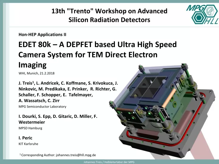
13th "Trento" Workshop on Advanced Silicon Radiation Detectors Hon-HEP Applications II EDET 80k – A DEPFET based Ultra High Speed Camera System for TEM Direct Electron Imaging WHI, Munich, 21.2.2018 J. Treis1, L. Andricek, C. Koffmane, S. Krivokuca, J. Ninkovic, M. Predikaka, E. Prinker, R. Richter, G. Schaller, F. Schopper, E. Tafelmayer, A. Wassatsch, C. Zirr MPG Semiconductor Laboratory I. Dourki, S. Epp, D. Gitaric, D. Miller, F. Westermeier MPSD Hamburg I. Peric KIT Karlsruhe 1 Corresponding Author: johannes.treis@hll.mpg.de Johannes Treis / Halbleiterlabor der MPG
Contents • Introduction to the instrument • DEPFET pixels • ASM • Module structure • System structure • CAD impressions • Summary & Outlook Johannes Treis / Halbleiterlabor der MPG
Introduction Stroboscopic imaging provides insight to the dynamics of processes Johannes Treis / Halbleiterlabor der MPG
Introduction "Normal" imaging: • Continuousillumination w/ fixedintensity • Exposureperiod"gated" byshutter • Exposure time definesimagecontrast • Tradeoffbetweenimagecontrastandimpactofmotionblur • Definedbythedynamicsofprocess "Stroboscopic" imaging: • Short, discreteilluminationperiodswith high intensity (flashbulb) • Pulse intensitydefinesimagecontrast • Decouplesexposure time, imagecontrastandmotionblur • Frequencyofilluminationdefines time resolution • Pulse durationdefinesimpactofmotionblur Johannes Treis / Halbleiterlabor der MPG
Introduction Stroboscopicimaging in TEM worldischallenging: • Stroboscopicillumination → Pulsedelectronsource • Real spaceimaging → Large sensitive area • High intensity → High dynamicrange • Directelectrondetection → Thinsubstrate • High pulse frequency → High framerate • "Grey scale" image → Nodatareductionpossible The instrument: • Detector FPA consistingof 4 individual, independentmodules ("tiles") capableof stand-aloneoperation. • Mounted in TEM focal plane (narrowenvironment) • Small sensitivitygapbetweentiles (1.2 mm) • DEPFET arrayswith 60 x 60 mm2pixelsize • Tilerraysize 512 x 512 pixels • 1 MPixelforcompleteFPA • Thinnedsubstratewith 50 mm and 30 mm thickness • ASM completewith passives and FEE (DCD / DMC) • Readout in rollingshuttermode • Readout time 100 ns / row, 4 rows in parallel → 12.8 ms / frame • Framerate max. 80 kHz • FEE allowsbufferingofbursts (movies) with 100 frames • Maximum burst rate 100 Hz Johannes Treis / Halbleiterlabor der MPG
Introduction • Data rate • Max. burstfrequency 100 Hz ( 100 frameseach) • DIgitizationwith 8 bitresolution • Tilemoduledata rate 2.9 GByte / s gross • Total data rate ~ 11.6 GByte /s gross • Data reduction / zerosuppressiondifficult Challenges: • Dynamic range • Single primaryelectronsensitivity • Primary electron @ 300 keV on 50 µm Si → Distinguish 8k e- fromnoise • 50 (better 100) primaries per pixeltoprovideenoughcontrast → 800k signalelectronstobestored in pixel • Operation in vacuum: • Small volume / extremelycompactsetup • Cooling / thermal stabilization • Multiple scattering: • Thin sensitive detectorsubstrate • Nosupportlayer • Highlyefficient beam dumpfortraversingelectons • Advanced thermal support Johannes Treis / Halbleiterlabor der MPG
DEPFET Pixel • DEPFET integratedamplifier • p-channel FET on depleted n-bulk • Signal chargecollected in potential minimumbelow FET channel • "Internal gate" • FET currentmodulation ≥ 300 pA/el. • Reset via clearFET • Low capacitance & noise • Charge storage, readout on demand • Rolling shutter mode EDET pixels: • Dynamic rangeproblem • Implementsignalcompression in pixel • Overflow tosourcetotailordynamicrange
DEPFET Pixel EDET pixels: • Shape ofsourceimplantcreates 2 overflowregions • Different onsetpointsofoverflow • Large dynamicrange • Sensor w/ integratedsignalcompression Drift DEPFET Gate (ext + int) Drain Clear Source Response curve (VDS = -5 V) Charge distribution (VGS = -3 V, VDS = -5 V) Drain current (100 µA) Overflow regions No additional deep-n drift field by wedge shape Signal charge (Me-) Secondary OF Primary OF Signal charge (Me-) Signal charge (Me-) Johannes Treis / Halbleiterlabor der MPG
Detector ASM ASM: • High integrationdensityrequiresintegrationofDetectormatrix, front-end ASICs andsupporting passives on commonsubstrate • "PCB on silicon" → All-Silicon module (ASM) • Substrate thinned down to 50 -30 µm thickness in sensorregion • Supportingwindowbars up to 8 serial links (@320 Mbit /s) … DirectCurrentDigitizerfor EDET (DCD-E) • UMC 130 nmtechnology • 256 channelsread in parallel • 8 bitdigitization, 100 nsconversion • 64 parallel dataoutput links @ 320 MBit/s DEPFET Movie Chip (DMC) • TSMC 40 nm technology • Data buffer, serializer & sequencer for all DCDs and Switchers • Fast data transfer to periphery using 8 parallel 320 Mbit /s LVDS outputs Switcher-B: • AMS H18 HV technology • Controller IC, 32 channels • Each channel driving gate and clear lines of 4 ASM pixel matrix rows in parallel Johannes Treis / Halbleiterlabor der MPG
Detector ASM JTAG Bias contacts Switcher Bank Pixel array 30.7 x 30. 7 mm2 Bondpads for DCD / DMC data & supplies Test pads (removed after met. 1 testing) Chip size ~ 50 x 38 mm2 DMC array DCD array (EDET specific DCD-E) Johannes Treis / Halbleiterlabor der MPG
ASM – bare die Johannes Treis / Halbleiterlabor der MPG
Module structure Module components: • ASM: All-Silicon module • Brick support: Mechanicaland thermal supportfor ASM andinterfacetomainheatsink • Patch panel: Wirebondadapter, local power conditioningandhousekeepingcircuitry • Integrated with 3 othertilemodules on mainheatsink in vacuumvessel • Vacuuminterfaceflangewithflexleadforelectricalconnection • Connectedto Module Interface circuitryforperipheralconnection • All hardwarecomponentsoftilemodule • Communication w/ control PC forhousekeepingand online monitoringusing 1 GBit Ethernet interface • Trigger inputfrom TEM andsynchronizationclock • Fileserver systemfor fast datastorage, datatransferusing 2 x 10 GBitopticalinterface (UDP stream) • Suppliedwith a single 12 V raw power supply Johannes Treis / Halbleiterlabor der MPG
Module structure Module Interface circuitry (MIC) : • Peripheralinterconnectbased on modular stackof 3 modules • MSM: Service modulehostingphysicalinterfaces & interconnects • Housekeeping & configuration • Fast datatransfer • Trigger inputs • Connectorsfor Mezzanine cards • MPM: Power modulehostingPreregulatorsandbiasingcircuitsfor ASM • Providesforsupplyofentiremodule w/ a single 12 V DC power supply • MBM: Brain modulebased on powerful ZynqUltraScale FPGA fromXilinx • Service functions, fast datatransferusing MGBTs and potential datacompressionandpreprocessing MBM module (Enclustra Mercury + XU1) Johannes Treis / Halbleiterlabor der MPG
System structure DAQ Concept: • Completesystemisformedby 4 identical, independenttilemodules • Configurationofmodules via individual standard 1Gb Ethernet link • Control PC doesconfiguration, housekeepingand online Monitoring • Trigger from TEM isappliedtoone ("master") module • Master distributesthetriggertoslavemodulesusingproprietary Inter-Module link (IML) • Fast dataistransferredtomodule-individual Fileserver storageusing 2 optical 10 Gbit Ethernet connections • Fileserver arraymakesdataavailablefor offline analysis • Possiblereplacementofmodule-individual configuration link by IML based master-slave architecture in a laterstage Johannes Treis / Halbleiterlabor der MPG
CAD impressions Cavity for beam dump • Brick support w/ patchpanelattached • Polysilicon for CTE-match Polysilicon brick • Beam dumpgeometryforlowestbackscattering Pitch adapter Johannes Treis / Halbleiterlabor der MPG
Hardware Johannes Treis / Halbleiterlabor der MPG
CAD impressions • Vacuumfeedthroughflange • Top viewof FPA w/o ASMs attached Johannes Treis / Halbleiterlabor der MPG
CAD impressions Insertion: • Insertion focomplete FPA stackfrombelow • Nocablemountingfrom top required after insertion Main heatsink • Complete FPA (4 ASMs, FEE shield not shown) Johannes Treis / Halbleiterlabor der MPG
Test program Prototyes: • Matrix prototypeswith 64 x 128 topologicalpixelsusedfordetectorand ASIC qualification, systemdevelopment • Current prototype assembliesusethe BELLE DHPT IC • Single pixelchipsfordetaileddeviceresponsecalibrationandirradiationtesting • Tests in progress • Test matrixassembly • Laser beam spot Johannes Treis / Halbleiterlabor der MPG
Summary & Outlook Status: • ASM pilotproductionfinished • Detectormeasurements on smalldevices in progress / qualificationof different designs • DCD-E availableandqualified • DMC submission 3/2018 • DLSP prototypingsuccessful • Roadmap for DLSP / MIC development • Fullsized prototype module in Q3/2018 • Using DHPT IC insteadof DMC • Full-scalesystemready Q1/2019 Johannes Treis / Halbleiterlabor der MPG
Backup slides Johannes Treis / Halbleiterlabor der MPG
Modulation transfer function Quantitative description for the contrast behavior Rainer Richter MPG Semiconductor Lab.
Thermal gradient 30 µm T ~ 11.3° • T ~ 12.1° T ~ 2.8° T ~ 11.7° T ~ 13.9 Detectortemperature: • Adaption ofoperationmodelimits thermal gradientovermatrixto 9°C (30 µm case) • Dutycycleof ~ 10:1 mandatorytokeeptemperaturegradientlow T ~ 2.7 ° Johannes Treis / Halbleiterlabor der MPG
Thermal gradient 50 µm T ~ 9.6° • T ~ 11.4° T ~ 3.3° T ~ 11.1° T ~ 13.9 Detectortemperature: • Adaption ofoperationmodelimits thermal gradientovermatrixto 7°C (50 µm case) • Dutycycleof ~ 10:1 mandatorytokeeptemperaturegradientlow T ~ 2.8 ° Johannes Treis / Halbleiterlabor der MPG
Thermal budget Johannes Treis / Halbleiterlabor der MPG
Radiation hardness MOS Operation window (100pe- limit) Real space detector sees a rather homogeneous radiation level → Oxide charge buildt up is homogeneous → compensated by Gate voltages Concern: inhomogeneous rad.
Scanning laser annealing Johannes Treis / Halbleiterlabor der MPG