Download
1 / 18
180 likes | 537 Views
Chapter 7. Register Transfer and Computer Operations. Design methodology To specify a large digital system with state table is very difficult. The large system is partitioned into modular subsystem, each of which performs some functional tasks.

E N D
Chapter 7. Register Transfer and Computer Operations • Design methodology • To specify a large digital system with state table is very difficult. • The large system is partitioned into modular subsystem, each of which performs some functional tasks. • The modules are constructed from such digital devices such as registers, counters, decoders, multiplexers, arithmetic elements, and control logic. • The various modules are interconnected by common data and control paths to form the digital computer system.
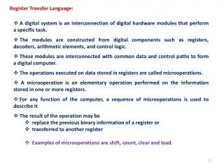
Register Transfer Operations (RTOs) • Digital modules are best defined by the registers they contain and the operations that are performed on the binary information stored in them. • Register operations: Shift, count, clear, load, etc. • The registers are assumed to be the basic components of the digital systems and the information flow and processing tasks among the data stored in the registers are referred as Register Transfer Operations.
Basic Components of RTOs • The set of registers in the system and their functions. • The operations that are performed with the information stored in the registers. • The control that supervises the sequences of operations in the system.
Registers, Operations and Control • Registers: We have known about them. • Operations: The operations performed on the information stored in registers are called micro-operations. A micro-operation is an elementary operation that can be performed in parallel on a string of bits during one clock pulse period. • A counter with parallel load can perform the micro-operations increment and load. • A bidirectional shift register can perform the shift right and shift left micro-operations. • The result of the operation may replace the previous binary information in a register or may be transformed to another register.
The control that initiates the sequence of operations consists of timing signals that sequence the operations in a pre-defined manner. • The outputs of the control logic are binary variables that initiate the various micro-operations in the registers.
Arithmetic Logic Unit and Shift Unit • In a computer system, we employ a number of storage registers and a common operational unit called arithmetic logic unit(ALU) to perform micro-operations. • To perform a micro-operation, • the contents of specified registers are placed in the inputs of ALU. • ALU performs specified operation. • The result is transferred to a destinational register. • The ALU is a combinational circuit so that the entire register transfer operation from the source registers through the ALU and into the destination register can be performed in one clock cycle. • The shift micro-operation are often performed in a shift register unit sometimes is considered as a part of the ALU.
Processor Unit and Central Processing Unit • A group of registers connected to a common ALU is called a processing unit. • The processing unit, when combined with a control unit that supervises the sequence of operations, is called Central Processing Unit (CPU). • Chapter 7 for Design of Processing Unit. • Chapter 8 for Design of Control Unit.
7.2 Register Transfer • Designation of registers: PC, R1, R2, IR, AR, … . (Fig. 7-1). • Register transfer with timing control • R2 R1: Transfer of the contents of register R1 into register R2. • T1: R2 R1: If (T1=1) then (R2 R1). • Basic symbols for register transfer. (Table 7-1) • Every register transfer notation implies a hardware implementation. (Fig. 7-2) • Exchange of the contents of R1 and R2 • T3: R2 R1, R1 R2 is possible by using edge-triggered flip-flops. • Multiplexer selection • If (T1=1) then (R0 R1) else if (T2=1) then (R0 R2) • Hardware implementation (Fig. 7-3)
7.3 Micro-operations • Four categories of micro-operations in digital computers: 1. Register transfer microoperations transfer binary information from one register to another. 2. Arithmetic microoperations perform arithmetic operations on numbers stored in registers. 3. Logic microoperations perform bit manipulation operations on non-numeric data stored in registers. 4. Shift microoperations perform shift operations on contents of registers. • 1st category don’t change the contents of registers. • 2nd, 3rd, and 4th categories change the contents of registers.
Basic arithmetic microoperations (Table 7-2) • Addition, subtraction, increment,decrement, and shift. • Hardware implementation of an arithmetic RTO (Fig. 7-4) X’T1: R1 R1 + R2 X’T1: R1 R2 + R2’ + 1 • Logic Microoperations (Table 7-3) • Example T1 + T2: R1 R2 + R3 , R4 R2 V R6 • AND Microoperation • It is used for cleaning to 0 a bit or a selected group of bits in a register. • Example R1: 10101101 10101011 R2: 00000000 10101011 R1 R2 R2: 00000000 10101011
OR microoperation • It is used to set to 1 a bit or a selected group of bits in a register. • Example R1: 10101101 10101011 R2: 11111111 00000000 R1 R1 V R2: 11111111 10101011 • Exclusive OR (XOR) microoperation • It is used to complement a bit or a group of bits in a register. ( , ) • Example • R1: 10101101 10101011 • R2: 11111111 00000000 • : 01010010 10101011
Shift microoperations • Shift microoperations are used for serial transfer of data. They are also used in arithmetic, logic and control operations. (Table 7-4) • Logical shift and rotate • Logical shift right (Fig. XX) • Logical shift left (Fig. XX) • Rotate right (Fig. XX) • Rotate left (Fig. XX) • Arithmetic shift • An arithmetic shift is a microoperation that shifts a signed binary number to the left or right. It must have the sign bit unchanged. • An arithmetic shift left multiplies a signed binary number by 2. (Fig. XX) • An arithmetic shift right divides a signed binary number by 2. (Fig. XX)
7-4 Bus Transfer • By fully connected lines between registers, need at least C(n,2) lines for each bit transfer, where n is the number of registers. • By a common bus, needs only one line for each bit transfer no matter how many registers we have. • Use multiplexers and decoders. (Fig. 7-6) • Use tri-state bus structure. (Fig. 7-7, 7-8, 7-9) • Memory transfer (Fig. 7-10)
7-5 Processor Unit • Processor unit = A set of registers + ALU (Fig. 7-11) • Processor unit is sometimes referred to as the data path because it forms the paths for the operations among registers. • Required control signals for processor unit • Control signals direct the information flow through the buses, the ALU, and the shifter by selecting various components in the processor unit. • Example: R1 R2 +R3 must have the control signals: 1. MUX A selector: Place the contents of R2 onto the bus. 2. MUX B selector: Place the contents of R3 onto bus. 3. ALU operation selector 4. Shift selector Decoder destination selector
7-6 Arithmetic Logic Unit (ALU) • A 4 bit ALU (Fig. 7-12) • The basic components of an arithmetic circuit in the parallel adder. (Fig. 7-13) • Function table (Table 7-5) • Circuit for one stage of arithmetic circuit (Fig. 7-14) • Logic diagram (Fig. 7-15) • Logic Circuit • Basic logic operations: AND, OR, XOR, and Complement • One stage of a logic circuit (Fig. 7-16) • Arithmetic logic unit (Fig. 7-17) • Function table for ALU (Table 7-6)
7-7 Shift Unit • The shifter unit attached to the bus system transfers the output of the ALU onto the output bus. • The basic operations for the shifter includes shift left, shift right, no shift, and output 0. • Function table for a shifter (Table 7-7) • 4-bit shifter (Fig. 7-18) • Barrel shifter (Fig. 7-19, Table 7-8) • A barrel shifter is a circuit that shifts the input data bits by a number of positions specified by the binary value of a set of selection lines. • The shift is a cyclic rotation which means that the input binary information is shifted in one direction and the bit coming from the most significant end of the shifter is brought back to the least significant position.
7-8 Control Word • The selection variables in a processor unit control the buses, the ALU, the shifter, and the destination register. • How do the control variables select the microoperations? (Fig. 7-20) • Encoding of control word (Table 7-9) • A control word of 16 bits is needed to specify a microoperation. • Example of control word (Table 7-10) • R1 R2-R3 Field: A B D F H Symbol: R2 R3 R1 F=A-B No shift Control word 010 011 001 101 000
A memory unit that stores control words is referred to as a control memory. • The output of the control memory is applied to the selection inputs of the processor. • By reading consecutive control words from memory, it is possible to initiate of microoperations for the processor. This type of control organization is called microprogramming.