Download
1 / 8
520 likes | 1.51k Views
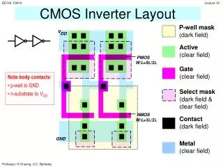
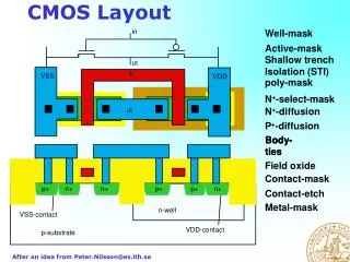
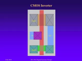
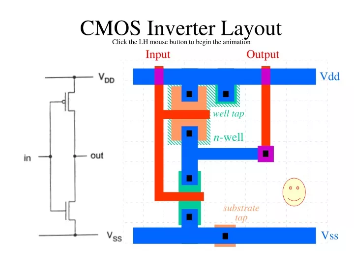
Vdd. n -well. Vss. CMOS Inverter Layout. Click the LH mouse button to begin the animation. Input. Output. well tap. substrate tap. Input. Output. Vdd. p+. metal. n-well. well tap. p+. polysilicon. n -well. p-substrate. polysilicon. n+. gate oxide. substrate tap. n+.

E N D
Vdd n-well Vss CMOS Inverter Layout Click the LH mouse button to begin the animation Input Output well tap substratetap
Input Output Vdd p+ metal n-well well tap p+ polysilicon n-well p-substrate polysilicon n+ gate oxide substratetap n+ field oxide Vss CMOS Inverter Structure
Input Output Vdd p+ metal n-well well tap p+ polysilicon n-well p-substrate polysilicon n+ gate oxide substratetap n+ field oxide Vss CMOS Inverter Structure
Polysilicon Design Rule Click the LH mouse button to begin the animation
Polysilicon Design Rule Input Output No overlap of channel. Insufficient overlap of cut.
Polysilicon Design Rule Input Output Faulty m1-pconnection Current not controlled by gate Current not controlled by gate
Polysilicon Design Rule Input Output Adequate overlap of channel. Sufficient overlap of cut.
Polysilicon Design Rule Input Output