Download
1 / 15
170 likes | 399 Views
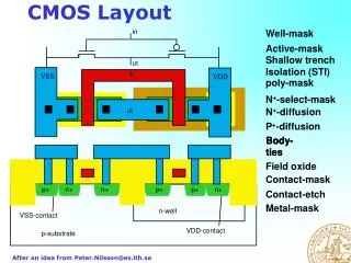
Layout of CMOS VLSI Circuits. Shmuel Wimer Bar Ilan Univ., School of Engineering. Simplified CMOS Process - Transistors. Metal P to N Connection. Serial Transistor Connection by Diffusion. Layout of Inverter. Layout of 2-Way NAND. 4-Way NAND Stick Layout.

E N D
Layout of CMOS VLSI Circuits Shmuel Wimer Bar Ilan Univ., School of Engineering CMOS VLSI Layout
Simplified CMOS Process - Transistors CMOS VLSI Layout
Metal P to N Connection CMOS VLSI Layout
Serial Transistor Connection by Diffusion CMOS VLSI Layout
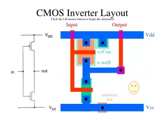
Layout of Inverter CMOS VLSI Layout
Layout of 2-Way NAND CMOS VLSI Layout
4-Way NAND Stick Layout CMOS VLSI Layout
Layout of Compound Gates – Euler Path CMOS VLSI Layout
Layout Styles CMOS VLSI Layout
130nm 90nm Layout in 130 and 90 Nanometers CMOS VLSI Layout
Layout in 90 and 65 Nanometers CMOS VLSI Layout
Layout in 65 Nanometers CMOS VLSI Layout
Layout in 65 and 45 Nanometers CMOS VLSI Layout
Possible Layout in 32 Nanometers CMOS VLSI Layout