Download
1 / 29
330 likes | 950 Views
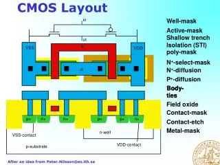
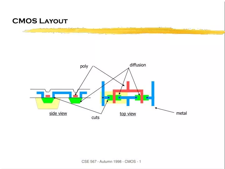
CMOS Layout. diffusion. poly. side view. metal. top view. cuts. A View of Interconnect Layers. Intel 4004 (1971). Pentium II (1996). Silicon in 2010. Die Area: 2.5x2.5 cm Voltage: 0.6 V Technology: 0.07 m. CMOS Inverter Layout. Layout. 4-input NAND gate.

E N D
CMOS Layout diffusion poly side view metal top view cuts CSE 567 - Autumn 1998 - CMOS - 1
A View of Interconnect Layers CSE 567 - Autumn 1998 - CMOS - 2
Intel 4004 (1971) CSE 567 - Autumn 1998 - CMOS - 3
Pentium II (1996) CSE 567 - Autumn 1998 - CMOS - 4
Silicon in 2010 Die Area: 2.5x2.5 cm Voltage: 0.6 V Technology: 0.07 m CSE 567 - Autumn 1998 - CMOS - 5
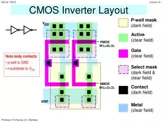
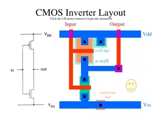
CMOS Inverter Layout CSE 567 - Autumn 1998 - CMOS - 6
Layout • 4-input NAND gate CSE 567 - Autumn 1998 - CMOS - 7
Standard Cell Design Methodology • Example “stick diagram” CSE 567 - Autumn 1998 - CMOS - 8
Different Layouts are Possible • Different layouts for x = CSE 567 - Autumn 1998 - CMOS - 9
The Barrel Shifter CSE 567 - Autumn 1998 - CMOS - 10
4x4 barrel shifter CSE 567 - Autumn 1998 - CMOS - 11
Logarithmic Shifter CSE 567 - Autumn 1998 - CMOS - 12
0-7 bit Logarithmic Shifter A 3 Out3 A 2 Out2 A 1 Out1 A 0 Out0 CSE 567 - Autumn 1998 - CMOS - 13
Latches CSE 567 - Autumn 1998 - CMOS - 14
Edge-Triggered Register (Master/Slave) CSE 567 - Autumn 1998 - CMOS - 15
Non-Overlapping Clocks CSE 567 - Autumn 1998 - CMOS - 16
Dynamic Register CSE 567 - Autumn 1998 - CMOS - 17
Registers and intervening logic • Switches and/or gates compute new values to store on next clock cycle straightforward implementation CL 2 1 this circuit can use the entire clock cycle – no wasted time - a form of retiming CL CL 2 1 CSE 567 - Autumn 1998 - CMOS - 18
Memory – Static Register Cells • 8-transistor cell bit bit' rd or wr (rd or wr)' sensing amplifier rd/wr' CSE 567 - Autumn 1998 - CMOS - 19
Memory – Dynamic Register Cells • 4-transistor cell data-in data-out' wr dedicated busses forreading and writing rd dynamic charge storagemust be refreshed CSE 567 - Autumn 1998 - CMOS - 20
Memory – Dynamic Register Cells (cont'd) • 3-transistor cell pre-charge data-out' togenerate 1 outputs data-in data-out' wr no p-type transistors yielda very compact cell rd CSE 567 - Autumn 1998 - CMOS - 21
Memory – Dynamic Register Cells (cont'd) precharge tointermediate voltage level • 1-transistor cell storage capacitoris one end of transistor charge sharing withbus capacitance(Ccell << Cbus) destructive read(must immediatelywrite back) extra demands onsense amplifier todetect small changesin bus charge CSE 567 - Autumn 1998 - CMOS - 22
Read-only Memory Cells • To store constants or other invariant data • Popular for control implementation bit1 bit2 bit3 read1 read2 programmable logic array structure (exploits distributed NOR gate structure) CSE 567 - Autumn 1998 - CMOS - 23
Multi-ported Register Cells • Add more input and output transistors (similar for all variations) • Not usually done for 1-transistor cells bus2' bus1 row-bus1 row-bus2 bus2 bus1' CSE 567 - Autumn 1998 - CMOS - 24
Random access memory • Decoding logic to select word • Attempt to make critical lines (data lines) as short as possible • Square aspect ratio rather than rectangular 2m k-bit words per row 2n by 2m*k bits decoder n memorycell array 2n rows addressof word(n+m bits) m multiplexer ( 2m :1) k bits wide (k bits/word) CSE 567 - Autumn 1998 - CMOS - 25
Decoders • Decoder looks like AND-plane of ROM(all input combinations) • usually replicatedthroughout array decoder memorycell array n rd/wr(row select) bit' bit CSE 567 - Autumn 1998 - CMOS - 26
Multiplexers • Decode address into one-hot control signals • Each bit passes through single n-device or pass gate note: bits of word in row are interleaved word1 word2 word3 word4 bit1 bit2 from a decoder CSE 567 - Autumn 1998 - CMOS - 27
m bits encoder contentaddressablememorycell array 2n rows n m Content-Addressable Memory • Compares input to all entries in memory in parallel • applications: pattern recognition, TLBs, etc. • Require and encoder to indicate where a match occurred • perform inverse function of decoders • take a one-hot collection of signals and encodes them CSE 567 - Autumn 1998 - CMOS - 28
Content-Addressable Memory Cells • Read and write like normal 6T memory cell • Match signal is precharged to 1, pulled to 0 if no match • send data on bit' and data' on bit for matching • match remains 1 if and only if all bits in word match rowselect match bit bit' CSE 567 - Autumn 1998 - CMOS - 29