Download
1 / 65
670 likes | 861 Views
The single cycle CPU. Performance of Single-Cycle Machines. Memory Unit 2 ns ALU and Adders 2 ns Register file (Read or Write) 1 ns Class Fetch Decode ALU Memory Write Back Total R-format 2 1 2 0 1 6

E N D
Performance of Single-Cycle Machines • Memory Unit 2 ns • ALU and Adders 2 ns • Register file (Read or Write) 1 ns Class Fetch Decode ALU Memory Write Back Total R-format 2 1 2 0 1 6 LW 2 1 2 2 1 8 SW 2 1 2 2 7ns Branch 2 1 2 5ns Jump 2 2ns
מה היה קורה עם cycleשל השעון היה באורך משתנה • נשווה לגבי תוכנית עם התערובת הבאה של פקודות: • Rtype: 44%, LW: 24%, SW: 12% • BRANCH: 18%, JUMP: 2% • I - מספר פקודות בתוכנית • T - אורך מחזור שעון • CPI - מספר מחזורים לפקודה = 1 Execution=I*T*CPI= 8*24%+7*12%+6*44%+5*18%+2*2%=6.3 ns
התוצאה EXE Single cycle T single clock * I T single clock 8 EXE Variable T variable clock * I T variable clock 6.3 יחס של 1.27. היחס יהיה יותר גרוע כאשר נממש פקודות מסובכות כמו פעולות עם floating point הפתרון: אינו שעון בגודל משתנה - מסובך מבחינת הבניה. הפתרון: פקודה לוקחת מספר משתנה של cycles.
Multicycle Approach הרעיון מאחורי שיטת ה- Multicycle: חיסכון בזמן: כל פקודה תקח את מספר היחידות השעון הנחוצות לה. חיסכון ברכיבים: שימוש באותו רכיב בשלבים שונים של הפקודה.
שיטת הבניה של ארכיטקטורת ה- Multicycle חלק את הפקודה לשלבים. כל שלב cycle: - אזן את כמות העבודה הנדרשת בכל שלב. - הקטן את כמות העבודה הנדרשת בכל שלב - כל שלב יבצע רק פעולה אחת פונקצינאלית. בסיום כל מחזור שעון: - שמור את הערכים עבור השלבים הבאים. - הוסף לביצוע משימה זו רגיסטרים פנימיים נוספים.
Timing of a lw instruction in a single cycle CPU PC 0x400000 I.Mem data Memory output Rs, Rt ALU inputs D.Mem adrs ALU output (address) D. Mem data Mem data We want to replace a long single CK cycle with 5 short ones: fetch execute memory decode Write back 2ns 1ns 2ns 2ns 1ns 0 1 2 3 4 5=(0) PC 0x400000 fetch Instruction in IR IR decode ALU calculates something A,B execute Timing of a lw instruction in a multi-cycle CPU ALUout Mem data memory MDR Write back
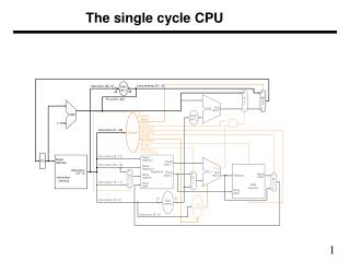
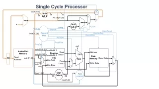
ck ck Therefore we should add registers to the single cycle CPU shown below: 4 Adder Reg File [25:21]=Rs 5 Data Memory Instruction Memory PC ALU [20:16]=Rt 5 Address D. Out 5 Rd D.In [15:0] 16 Sext 16->32
ck ck ck ck ck ck ck Adding registers to “split” the instruction to 5 stages: 4 Adder A Reg File ALUout MDR [25:21]=Rs 5 Data Memory Instruction Memory PC ALU IR [20:16]=Rt 5 Address D. Out 2 5 Rd D.In PCWrite B 4 3 0 1 5 [15:0] 16 Sext 16->32
Here is the book’s version of the multi-cycle CPU: Only PC and IR have write enable signals All other registers hold data for a single cycle
IR[20:16]=Rt IR[25:21]=Rs 5 5 ck ck ck ck ck ck Here is our version of A mult--cycle CPU capable of R-type & lw/sw & branch instructions Reg File A Instruction & data Memory PC ALUout IR ALU 5 Rd B 4 IR[15:0] 16 Sext 16->32 << 2 <<2 IR
Let us explain the multi-cycle CPU • First we’ll look at a CPU capable of performing only R-type instructions • Then, we’ll add the lw instruction • And the sw instruction • Then, the beq instruction • And finally, the j instruction
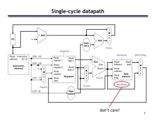
PC 0x400000 0x400004 Memory output New Memory output Rs, Rt ALU inputs new ALU inputs ALU output New ALU output Write back fetch execute decode [15:11]=Rd [20:16]=Rt [25:21]=Rs 5 5 5 ck ck Let us remind ourselves how works a single cycle CPU capable of performingR-type instructions.Here you see the data-path and the timing of an R-typeinstruction. 4 Adder [31:26] 6 Reg File Instruction Memory PC ALU [5:0]=funct 6
[25:21]=Rs [20:16]=Rt [15:11]=Rd 5 5 5 ck ck A single cycle CPU demo: R-type instruction 4 Instruction Memory Reg File ALU PC
ck ck ck ck ck A multi cycle CPU capable of performing R-type instructions Reg File A IR[25:21]=Rs 5 Instruction & data Memory PC ALUout IR ALU IR[20:16]=Rt 5 5 Rd B
ck ck ck ck ck A multi cycle CPU capable of R-type & instructionsfetch Reg File A IR[25:21]=Rs 5 Instruction & data Memory PC ALUout IR ALU IR[20:16]=Rt 5 5 Rd B 0 1
ck ck ck ck ck A multi cycle CPU capable of R-type & instructionsdecode Reg File A IR[25:21]=Rs 5 Instruction & data Memory PC ALUout IR ALU IR[20:16]=Rt 5 5 Rd B 1 2
ck ck ck ck ck A multi cycle CPU capable of R-type & instructionsexecute Reg File A IR[25:21]=Rs 5 Instruction & data Memory PC ALUout IR ALU IR[20:16]=Rt 5 5 Rd B 3 2
ck ck ck ck ck ck A multi cycle CPU capable of R-type & instructionswrite back Reg File A IR[25:21]=Rs 5 Instruction & data Memory PC ALUout IR ALU IR[20:16]=Rt 5 Rd 5 Rd B 3 4
PC 0x400000 Inst. Mem data Memory output = the instruction Timing of an R-type instruction in a single cycle CPU Rs, Rt ALU inputs ALU output (Data = result of cala.) GPR input fetch execute Write Back decode 0 1 2 3 4 (=0) PC Mem data Timing of an R-type instruction in a multi-cycle CPU fetch Previous inst. Current instruction IR decode A,B execute ALUout Write back
fetch PC Mem data Current instruction IR=M ( PC ) Previous inst. Current instruction next inst. IR decode GPR outputs A= Rs, B= Rt A,B execute ALU output ALUuot= A op B Write back Rd = ALUout ALUout At the rising edge of CK: Rd=ALUout R-Type instruction takes 4 CKs IRWrite The state diagram: A= Rs, B= Rt ALUout = A op B IR=M(PC) Rd=ALUout
IR[20:16]=Rt IR[25:21]=Rs 5 5 ck ck ck ck ck A multi-cycle CPU capable of R-type instructions (PC calc. ) Reg File A Instruction & data Memory PC ALUout IR ALU 5 Rd B 4
fetch current PC next PC = current PC+4 PC Mem data IR Previous inst. current instruction next inst. decode GPR outputs A,B execute ALU output Write back ALUout At the rising edge of CK: Rd=ALUout ALUuot = A op B PC = PC+4 PCWrite
ck ck ck ck ck A multi cycle CPU capable of R-type & instructionsfetch Reg File A IR[25:21]=Rs 5 Instruction Memory PC ALUout IR ALU ALU IR[20:16]=Rt 5 5 Rd B 4
The state diagram of a CPU capable of R-type instructions only Fetch 0 Decode 1 R-type ALU 6 WBR 7 IR=M(PC) PC = PC+4 A=Rs B=Rt ALUout=A op B Rd = ALUout
The state diagram of a CPU capable of R-type and lw instructions Fetch 0 Decode 1 lw R-type AdrCmp ALU 2 WB 6 lw Load 3 WBR 4 7 ALUout= A+sext(imm) MDR = M(ALUout) Rt = MDR
ck ck ck ck ck ck ck We added registers to “split” the instruction to 5 stages.Let’s discuss the lw instruction 4 Adder A Reg File ALUout MDR [25:21]=Rs 5 Data Memory Instruction Memory PC ALU IR [20:16]=Rt 5 Address D. Out 2 5 Rd D.In PCWrite B 4 3 0 1 5 [15:0] 16 Sext 16->32
IR[20:16]=Rt IR[25:21]=Rs 5 5 ck ck ck ck ck ck First we draw a multi-cycle CPU capable of R-type & lw instructions: Reg File A Instruction Memory PC ALUout IR ALU ALU ALU 5 Rd B 4 IR[15:0] 16 Sext 16->32 Data Memory MDR We just moved the data memory All parts related to lw only are blue
IR[25:21]=Rs IR[20:16]=Rt 5 5 ck ck ck ck ck ck A multi-cycle CPU capable of R-type & lw instructionsfetch Reg File A Instruction Memory PC ALUout IR ALU ALU ALU 5 Rd B 4 IR[15:0] 16 Sext 16->32 Data Memory MDR
ck ck ck ck ck ck A multi-cycle CPU capable of R-type & lw instructionsdecode Reg File A IR[25:21]=Rs 5 Instruction Memory PC ALUout IR ALU IR[20:16]=Rt 5 5 Rd B 4 IR[15:0] 16 Sext 16->32 << 2 Data Memory MDE
IR[20:16]=Rt IR[25:21]=Rs 5 5 ck ck ck ck ck ck A multi-cycle CPU capable of R-type & lw instructionsAdrCmp Reg File A Instruction Memory PC ALUout IR ALU ALU 5 Rd B 4 IR[15:0] 16 Sext 16->32 Data Memory MDR
IR[25:21]=Rs IR[20:16]=Rt 5 5 ck ck ck ck ck ck A multi-cycle CPU capable of R-type & lw instructionsmemory Branch Address Reg File A InstructionMemory PC ALUout IR ALU 5 Rd B 4 IR[15:0] 16 Sext 16->32 << 2 Data Memory MDR
IR[25:21]=Rs IR[20:16]=Rt 5 5 ck ck ck ck ck ck ck A multi-cycle CPU capable of R-type & lw instructionsWB Reg File A InstructionMemory PC ALUout IR ALU Rt 5 Rd B 4 IR[15:0] 16 Sext 16->32 Data Memory MDR
IR[20:16]=Rt IR[25:21]=Rs 5 5 ck ck ck ck ck ck ck Can we unite the Instruction & Data memories? (They are not used simultaneously as in the single cycle CPU) Reg File A InstructionMemory PC ALUout IR ALU 5 Rd B 4 IR[15:0] 16 Sext 16->32 Data Memory MDR
IR[20:16]=Rt IR[25:21]=Rs 5 5 ck ck ck ck ck ck So here is a multi-cycle CPU capable of R-type & lw instructionsusing a single memory for instructions & data Reg File A Instruction & data Memory PC ALUout IR ALU 5 Rd B 4 IR[15:0] 16 Sext 16->32 MDR
PC 0x400000 I.Mem data Memory output Timing of a lw instruction in a single cycle CPU Rs, Rt ALU inputs D.Mem adrs ALU output (address) D. Mem data Mem data fetch execute memory decode Write back PC PC+4 fetch current instruction IR Previous inst. Timing of a lw instruction in a multi-cycle CPU decode A,B execute Data address ALUout Mem data memory Data to Rt MDR Write back
fetch PC IR=M ( PC ) PC= PC+4 Mem data IR Previous inst. current instruction decode GPR outputs A= Rs, B= Rt A,B execute ALU output Data address ALUuot= A+sext(imm) ALUout Data address memory Mem data MDR=M(ALUout) Write back Data to Rt MDR At the rising edge of CK: Rt=MDR PCWrite, IRWrite
The state diagram of a CPU capable of R-type and lw instructions WB IR=M(PC) PC = PC+4 Fetch 0 A=Rs B=Rt Decode 1 lw R-type ALUout= A+sext(imm) AdrCmp ALU ALUout=A op B 2 6 Load MDR = M(ALUout) 3 WBR Rt = MDR Rd = ALUout 4 7
IR[25:21]=Rs IR[20:16]=Rt 5 5 ck ck ck ck ck ck A multi-cycle CPU capable of R-type & lw & sw instructions Branch Address Reg File A Instruction & data Memory PC ALUout IR ALU 5 Rd B 4 IR[15:0] 16 Sext 16->32 << 2 MDR lw sw
The state diagram of a CPU capable of R-type and lw and sw instructions Fetch 0 Decode 1 lw+sw R-type AdrCmp ALU 2 WB 6 lw sw Load Store 3 5 WBR 4 7 IR=M(PC) PC = PC+4 A=Rs B=Rt ALUout= A+sext(imm) ALUout=A op B M(ALUout)=B MDR = M(ALUout) Rd = ALUout Rt = MDR
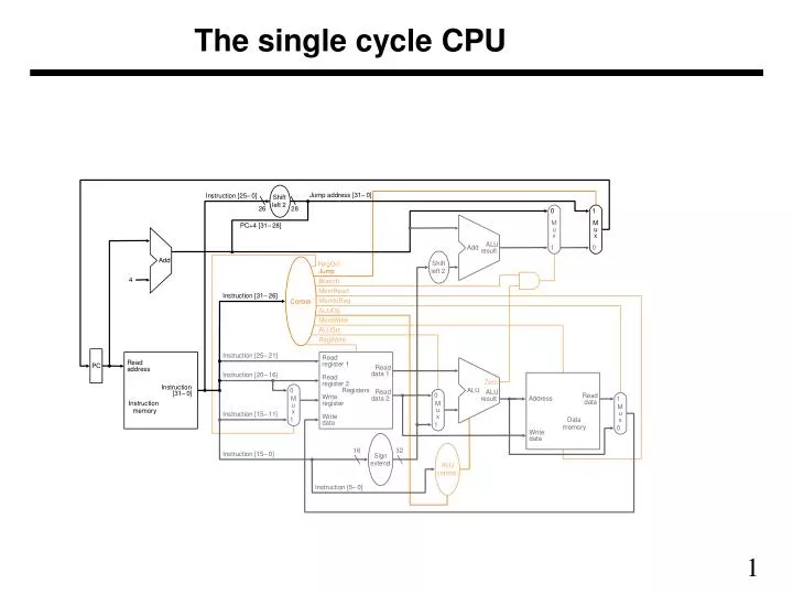
IR[20:16]=Rt IR[25:21]=Rs 5 5 ck ck ck ck ck ck A multi-cycle CPU capable of R-type & lw/sw & branch instructions Reg File A Instruction & data Memory PC ALUout IR ALU 5 Rd B 4 IR[15:0] 16 Sext 16->32 << 2 <<2 IR
Adding the instruction beq to the state diagram: Fetch 0 Decode 1 lw+sw beq R-type AdrCmp Branch ALU 2 8 WB 6 lw sw zero Load not zero Store 3 5 WBR 4 7 Calc Rs -Rt (just to produce the zero signal) Calc PC=PC+sext(imm)<<2
Fetch 0 Calc ALUout=PC+sext(imm)<<2 Decode 1 lw+sw beq R-type AdrCmp Branch ALU 2 8 WB 6 lw sw Load Store 3 5 WBR 4 7 Adding the instruction beq to the state diagram, a more efficient way: Let’s use the decode state in which the ALU is doing nothing to compute the branch address.We’ll have to store it for 1 more CK cycle, until we know whether to branch or not! (We store it in the ALUout reg.) Calc Rs - Rt. If zero, load the PC with ALUout data, else do not load the PC
IR[25:21]=Rs IR[20:16]=Rt 5 5 ck ck ck ck ck ck A multi-cycle CPU capable of R-type & lw/sw & branch instructions PC+4 Reg File A Instruction & data Memory PC ALUout IR ALU 5 Rd B 4 IR[15:0] 16 Sext 16->32 <<2 IR Branch Address
Adding the instruction j to the state diagram: WB Fetch 0 Decode 1 j lw+sw beq R-type Jump AdrCmp Branch ALU 9 2 8 6 lw sw Load Store 3 5 WBR 4 7 PC = PC[31:28] || IR[25:0]<<2
IR[20:16]=Rt IR[25:21]=Rs 5 5 ck ck ck ck ck ck A multi-cycle CPU capable of R-type & lw/sw & branch & jump instructions PC+4= next address IR[25:0] Jump address <<2+ PC[31:28] Reg File A Instruction & data Memory PC ALUout IR ALU 5 Rd B 4 IR[15:0] 16 Sext 16->32 <<2 IR Branch Address
סיכום שלבי הפקודות השונות 0 1 6 2 8 9 3 7 4 5
The final state diagram: WB Fetch 0 Decode 1 j lw+sw beq R-type Jump AdrCmp Branch ALU 9 2 8 6 lw sw Load Store 3 5 WBR 4 7