Download
1 / 15
150 likes | 324 Views
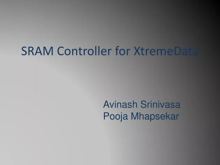
SRAM Controller for XtremeData. Avinash Srinivasa Pooja Mhapsekar. XtremeData Machine. App FPGA A. These two FPGAs have the user design. App FPGA B. Bridge FPGA. Used for communication between the app FPGAs and the system memory. Xtremedata. Allows 4MB of data to be sent at a time

E N D
SRAM Controller for XtremeData AvinashSrinivasa PoojaMhapsekar
App FPGA A These two FPGAs have the user design App FPGA B Bridge FPGA Used for communication between the app FPGAs and the system memory.
Xtremedata • Allows 4MB of data to be sent at a time • The next 4MB can be sent only after some data has been received. • The SW code should specify the number of bytes to be received. • 8 MB of quad data rate SRAM for each FPGA.
TOP TU Current Design 256 bits FIFO System Memory 8 bits Bridge FPGA Data_out DESIGN Data_in 8 bits FIFO 256 bits
MOTIVATION • Bio-informatics application running on hardware generates 1 GB of output data for every 4 MB of input data sent by software. • Hardware can send 4 MB of data back to software and carry on processing but has to wait for next chunk of data from software before sending again. • Software attempts to send the next chunk but not able to because processing of the previous chunk is still not complete. • Hardware and is now ready with the next 4 MB but is not able to send since data has not arrived from software. • DEADLOCK caused since hardware and software are both waiting on each other.
System Memory Bridge FPGA Application FPGA 4 MB 1 MB 1 MB 1 MB 1 MB 1 MB 1 MB 250 MB Output data To System Memory 4 MB of output data sent 246 MB of data to be stored
System Memory Bridge FPGA Application FPGA Softwareattempts 1 MB 1 MB 1 MB 1 MB 1 MB to send next 4 MB Another 250 MB of output data generated To System Memory Cannot send the next output chunk Waiting for software Not enough resources to store (?)
SOLUTION • Write all the software data into memory (SRAM) and have the hardware receive it from there -> solves the problem of input FIFO being full. • Have software do a series of dummy writes until the entire 1 GB of data generated is sent by hardware. • Software can send the next chunk of real data now to the SRAM and the cycle is repeated until all the data from software has been processed.
SRAM (4 MB stored) 4 MB data Bridge FPGA System Memory Application FPGA 1 MB 250 MB Output data To System Memory 4 MB of output data sent
SRAM (4 MB stored) data Bridge FPGA System Memory Application FPGA Dummy write onto register 1 MB 250 MB Output data To System Memory Next 4 MB of output data sent
SRAM CONTROLLER • The SRAM operates at 300 MHz while the controller is operating at 150 MHz. • The controller interfaces with the SRAM through the QDR port to write to and read from it. • Since it’s a quad-data rate, the port takes 144 bit data from the controller and gives it to the memory in 4 chunks of 36 bits each, all in one clock cycle. • The controller reads 128 bit data from the input FIFO and pads it with zeroes appropriately to convert it into 144 bit while writing. • While reading from the SRAM, converts the 144 bit data back to 128 bit and feeds it to the design.
TU TOP Modified Design DESIGN SRAM 8 bits System Memory FIFO QDR2 PORT 144 bits Control signals 144 bits 128 bits data in data out CONTROLLER 128 bits Bridge FPGA Data_in FIFO 256 bits