Download
1 / 1
70 likes | 730 Views
2013/9/2 HSTD9-ID54. Potential in bulk, 2D display. p-stop. Silicon avalanche breakdown voltage ~300 kV/cm. n + -Implant. n + -Implant. Location of bias voltage breakdown in n-in-p silicon segmented sensors with p-stop structure before and after irradiation. Backplane (-200 V).

E N D
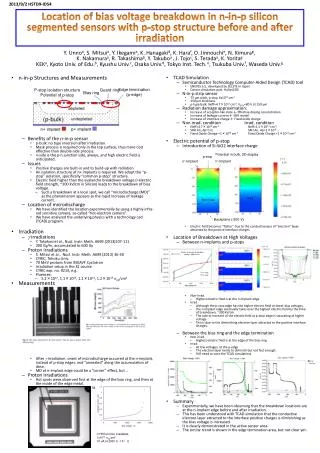
2013/9/2 HSTD9-ID54 Potential in bulk, 2D display p-stop Silicon avalanche breakdown voltage ~300 kV/cm n+-Implant n+-Implant Location of bias voltage breakdown in n-in-p silicon segmented sensors with p-stop structure before and after irradiation Backplane (-200 V) Y. Unnoa, S. Mitsuia, Y. Ikegamia, K. Hanagakid, K. Haraf, O. Jinnouchie, N. Kimurag, K. Nakamuraa, R. Takashimab, Y. Takuboa, J. Tojoc, S. Teradaa, K. Yoritag KEKa, Kyoto Univ. of Edu.b, Kyushu Univ.c, Osaka Univ.d, Tokyo Inst. Tech. e, Tsukuba Univ.f, WasedaUniv.g • n-in-p Structures and Measurements • Benefits of the n-in-p sensor • p-bulk: no type inversion after irradiation. • Mask process is required only in the top surface, thus more cost effective than double-side process. • n-side is the p-n junction side, always, and high electric field is anticipated. • Issues • Positive charges are built-in and to build-up with radiation. • An isolation structure of n+ implants is required. We adopt the “p-stop” isolation, specifically “common p-stop” structure. • Electric field higher than the avalanche breakdown voltage (=electric field strength, ~300 kV/cm in Silicon) leads to the breakdown of bias voltage. • Such a breakdown at a local spot, we call “microdischarge (MD)” as the phenomenon appears as the rapid increase of leakage current. • Location of microdischarge • We have identified the location experimentally by using a highly infra-red sensitive camera, so-called “hot-electron camera”. • We have analyzed the underlying physics with a technology cad (TCAD) program. • Irradiation • g irradiations • Y. Takahasi et al., Nucl. Instr. Meth. A699 (2013)107-111 • 200 Gy/hr, accumulated to 600 Gy • Proton irradiations • S. Mitsui et al., Nucl. Instr. Meth. A699 (2013) 36-40 • CYRIC, Tohoku Univ. • 70 MeV protons from 930AVF Cyclotron • Irradiation setup in the 32 course • CYRIC exp. no. 9214, e.g. • Fluences: • 5.2×10¹², 1.1×10¹³, 1.2×10¹⁴, 1.2×10¹⁵neq/cm2 • Measurements • girradiations • After g irradiation, onset of microdischargeoccurred at the n-implant, instead of p-stop edges, and “annealed” along the accumulation of dose. • MD at n-implant edge could be a “corner” effect, but … • Proton irradiations • Hot spots were observed first at the edge of the bias ring, and then at the inside of the edge metal. • The highest electric field is at the bias ring (n+ implant), not at the edge ring (p+ implant). • TCAD Simulation • Semiconductor Technology Computer-Aided Design (TCAD) tool • ENEXSS 5.5, developed by SELETE in Japan • Device simulation part: HyDeLEOS • N-in-p strip sensor • 75 µm pitch, p-stop 4x1012 cm-2 • 150 µm thickness • p-type bulk, Neff=4.7×1012 cm-3, VFDV=80 V at 150 µm • Radiation damage approximation: • Increase of acceptor-like state ← Effective doping concentration • Increase of leakage current ← SRH model • Increase of interface charge ← Fixed oxide charge • Non irrad. condition Irrad. condition • Neff=4.7×1012 cm-3 Neff=1.5×1013 cm-3, • SRH An, Ap=1.0, SRH An, Ap=1×10⁻⁸, • Fixed Oxide Charge =1×1010 cm-2Fixed Oxide Charge =1×1012 cm-2 • Electric potential of p-stop • Introduction of Si-SiO2 interface charge • Electric field becomes “flatter” due to the conductiveness of “electron” layer attracted to the positive interface charges. • Location of Breakdown at High Voltages • Between n-implants and p-stops • Non-irrad. • Highest electric field is at the n-implant edge • Irrad. • Although the p-stop edge has the higher electric field at lower bias voltages, • the n-implant edge eventually takes over the highest electric field by the time of breakdown, ~300 kV/cm. • The rate to increase of the electric field at p-stop edge is saturating at higher voltage. • This is due to the diminishing electron layer attracted to the positive interface charges. • Between the bias ring and the edge termination • Non-irrad. • Highest electric field is at the edge of the bias ring. • Irrad. • At low voltages, at the p-edge • The electron layer tends to diminish but not fast enough. • Still need to tune the TCAD simulations. • Summary • Experimentally, we have been observing that the breakdown locations are at the n-implant edge before and after irradiation. • This has been understood with TCAD simulation that the conductive electron layer attracted to the interface positive charges is diminishing as the bias voltage is increased. • It is clearly demonstrated in the active sensor area. • The similar trend is shown in the edge termination area, but not clear yet. Edge termination (p-edge) P-stop isolation structure Potential of p-stop Guard ring Bias ring irrad. Non-irrad. Bias voltage -1700V Bias voltage -1700V density CYRIC proton irradiated, 1x10¹⁴neq/cm2 10 uA at 2000 V, -15 °C