Download
1 / 1
10 likes | 162 Views
Temperature effects on the growth and electrical properties of Er 2 O 3 films on Ge substrates. T. Ji 1 , T. X. Nie 1 , J. Cui 1 , Z. B. Fang 2 , X. J. Yang 1 , Y. L. Fan 1 , Z. Y. Zhong 1 , and Z. M. Jiang 1 1 State Key Laboratory of Surface Physics, Fudan University, Shanghai 200433, China

E N D
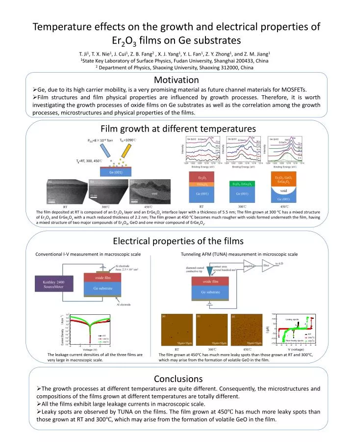
Temperature effects on the growth and electrical properties of Er2O3 films on Ge substrates T. Ji1, T. X. Nie1, J. Cui1, Z. B. Fang2 , X. J. Yang1, Y. L. Fan1, Z. Y. Zhong1, and Z. M. Jiang1 1State Key Laboratory of Surface Physics, Fudan University, Shanghai 200433, China 2 Department of Physics, Shaoxing University, Shaoxing 312000, China • Motivation • Ge, due to its high carrier mobility, is a very promising material as future channel materials for MOSFETs. • Film structures and film physical properties are influenced by growth processes. Therefore, it is worth investigating the growth processes of oxide films on Ge substrates as well as the correlation among the growth processes, microstructures and physical properties of the films. Film growth at different temperatures The film deposited at RT is composed of an Er2O3 layer and an ErGexOy interface layer with a thickness of 5.5 nm; The film grown at 300 ℃ has a mixed structure of Er2O3 and ErGexOy with a much reduced thickness of 2.2 nm; The film grown at 450 ℃ becomes much rougher with voids formed underneath the film, having a mixed structure of two major compounds of Er2O3, GeO and one minor compound of ErGexOy. Electrical properties of the films Conventional I-V measurement in macroscopic scale Tunneling AFM (TUNA) measurement in microscopic scale The leakage current densities of all the three films are very large in macroscopic scale. The film grown at 450℃ has much more leaky spots than those grown at RT and 300℃, which may arise from the formation of volatile GeO in the film. • Conclusions • The growth processes at different temperatures are quite different. Consequently, the microstructures and compositions of the films grown at different temperatures are totally different. • All the films exhibit large leakage currents in macroscopic scale. • Leaky spots are observed by TUNA on the films. The film grown at 450℃ has much more leaky spots than those grown at RT and 300℃, which may arise from the formation of volatile GeO in the film.