Download
1 / 2
20 likes | 133 Views
Growth and Optical Properties of Nonpolar m -plane GaN on Patterned Si and Sapphire Substrates Hadis Morko ç, Virginia Commonwealth University, DMR 0907096.

E N D
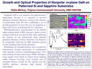
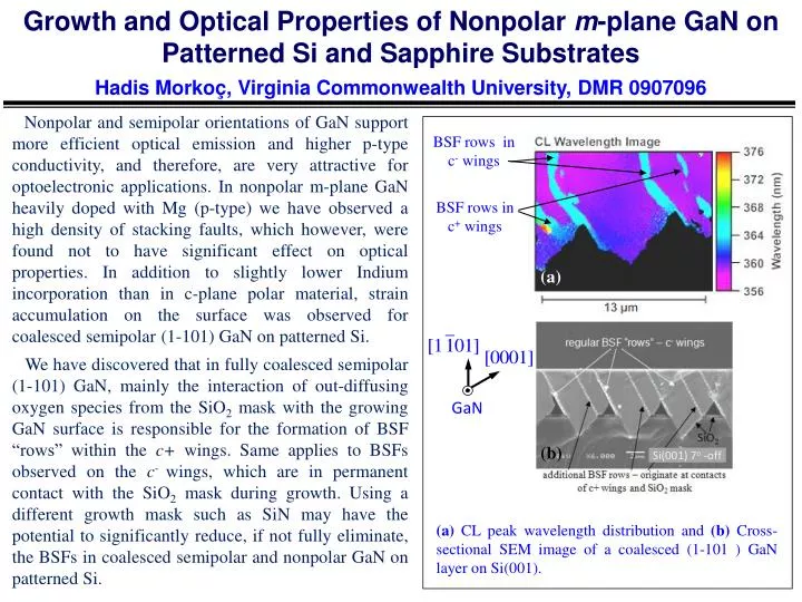
Growth and Optical Properties of Nonpolar m-plane GaN on Patterned Si and Sapphire Substrates Hadis Morkoç, Virginia Commonwealth University, DMR 0907096 Nonpolar and semipolar orientations of GaN support more efficient optical emission and higher p-type conductivity, and therefore, are very attractive for optoelectronic applications. In nonpolar m-plane GaN heavily doped with Mg (p-type) we have observed a high density of stacking faults, which however, were found not to have significant effect on optical properties. In addition to slightly lower Indium incorporation than in c-plane polar material, strain accumulation on the surface was observed for coalesced semipolar (1-101) GaN on patterned Si. We have discovered that in fully coalesced semipolar (1-101) GaN, mainly the interaction of out-diffusing oxygen species from the SiO2 mask with the growing GaN surface is responsible for the formation of BSF “rows” within the c+ wings. Same applies to BSFs observed on the c-wings, which are in permanent contact with the SiO2 mask during growth. Using a different growth mask such as SiN may have the potential to significantly reduce, if not fully eliminate, the BSFs in coalesced semipolar and nonpolar GaN on patterned Si. BSF rows in c- wings BSF rows in c+ wings (a) GaN (b) Si(001) 7o -off (a) CL peak wavelength distribution and (b) Cross-sectional SEM image of a coalesced (1-101 ) GaN layer on Si(001).
Growth and Optical Properties of Nonpolar m-plane GaN on Patterned Si and Sapphire Substrates Hadis Morkoç, Virginia Commonwealth University, DMR 0907096 This project provided the graduate students an excellent opportunity for cross-disciplinary learning in a collaborative research environment involving US and international universities and industry. Spatially resolved CL measurements were performed by undergraduate student C. Karbaum and graduate student S. Metzner from Prof. Jürgen Christen’s group at the Otto-von-Guericke University Magdeburg, Germany, and p-type Mg doping of m-plane GaN was studied in collaboration with Linköping University, Sweden, and with Kyma Technologies, Inc., USA. Moreover, this project allowed training of a VCU undergraduate student, Tyler Selden, for surface characterization using AFM. Tyler Selden studied systematically the surfaces of nonpolar and semipolar GaN films to identify the effects of growth conditions on film morphology and strain. (a) (b) [0001] SiO2 10 m Si(001) 7o -off substrate (a) Inclined SEM image of semipolar (1-101) GaN layer grown on Si(001) patterned substrate. (b) AFM image of 4 μm x 4 μm area of the GaN layer shown in (a); vertical range is 7 nm, rms is 0.791 nm. Atomic steps clearly seen on the AFM image are indicative of step-flow growth mode. * The AFM image was collected by VCU undergraduate student Tyler Selden.