Avalanche Photodiode Characterization
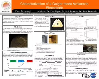
Avalanche Photodiode Characterization. David Hutchinson Semiconductor Devices and Models I Mid-Term Presentation - 10/14/2010. Impact Ionization. Multiplication Factor. For low frequency and equal ionization coefficients the multiplication is: M=1/(1- α W d )

Avalanche Photodiode Characterization
E N D
Presentation Transcript
Avalanche Photodiode Characterization David Hutchinson Semiconductor Devices and Models I Mid-Term Presentation - 10/14/2010
Multiplication Factor • For low frequency and equal ionization coefficients the multiplication is: • M=1/(1-αWd) • Where α = ionization rate and Wd = Depletion Width
Multiplication Noise Factor • F(M) = M*[1-(1-K)((M-1)/M)^2] • Multiplication noise depends on the ratio of ionization coefficients • Can either have either Electron or Hole injection (αp/ αn or αn/αp) • Where in the depletion region the carrier is created will determine which carrier is injected • The noise is small of the difference between the ionization coefficients is large
Applications • Fiber Optics/Night Vision • Laser Range Finding and Laser Guidance • Positron Emission Tomography (PET) and Single Photon Counting for particle physics experiments • Materials – Si, Ge, HgCdTe, InGaAs, GaN
Experimental Plans • Measure the temperature dependence of a Hamamatsu APDs photo response • This will be accomplished using a Cryostat, laser diode, function generator, and lock-in amplifier.
Simulation Plans • MEDICI will be used to simulate the behavior of an Avalanche Photodiode • The doping profile of Commercial photodiodes such as the Hamamatsu to be used in the experimental section are not well published • The profile will be estimated and adjusted based on results
How to Estimate the Doping Profile • We know the basic strength of the fields necessary to produce impact ionization, to that tells us the relative doping intensities required. • Their distribution can be estimated based on a basic analysis of the diode’s spectral response
Spectral Response Analysis • We know that carriers that experience gain must be created in the space charge region, or at least have the opportunity to drift into the space charge region. • The relative response over the visible spectrum should give us an estimate of the size and depth of the space charge region.
Backup Plans • In the event that the cryostat is not operational in time for the final project, there are 2 other physical characterizations to consider • Spectral Response – Halogen Source/Monochromator • Surface Response – Focused laser/Motion Controllers
Backup Plans • There is one problem with these techniques, they require the devices to be calibrated, which is traditionally done with the same diodes which are to be tested. • Another alternative is to use APSYS, another finite element modeling software, and do a comparison between the results it produces and MEDICI

