Download

1 / 76
2.16k likes | 5.37k Views
555 TIMER. 555 Timer. Introduction: The 555 Timer is one of the most popular and versatile integrated circuits ever produced! “ Signetics ” Corporation first introduced this device as the SE/NE 555 in early 1970. It is a combination of digital and analog circuits.

E N D
555 Timer Introduction: • The 555 Timer is one of the most popular and versatile integrated circuits ever produced! • “Signetics” Corporation first introduced this device as the SE/NE 555 in early 1970. • It is a combination of digital and analog circuits. • It is known as the “time machine” as it performs a wide variety of timing tasks. • Applications for the 555 Timer include: • Ramp and Square wave generator • Frequency dividers • Voltage-controlled oscillators • Pulse generators and LED flashers
555 timer- Pin Diagram The 555 timer is an 8-Pin D.I.L. Integrated Circuit or ‘chip’ Notch Pin 1
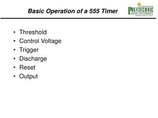
Best treated as a single component with required • input and output OUTPUT PROCESS INPUT 555 Timer • Description: • Contains 25 transistors, 2 diodes and 16 resistors • Maximum operating voltage 16V • Maximum output current 200mA If you input certain signals they will be processed / controlled in a certain manner and will produce a known output.
Inside the 555 Timer + Truth Table Vref Threshold Control Voltage R Q - Q S Trigger Discharge Fig: Functional Diagram of 555 Timer
Inside the 555 Timer Operation: • The voltage divider has three equal 5K resistors. It divides the input voltage (Vcc) into three equal parts. • The two comparators are op-amps that compare the voltages at their inputs and saturate depending upon which is greater. • The Threshold Comparator saturates when the voltage at the Threshold pin (pin 6) is greater than (2/3)Vcc. • The Trigger Comparator saturates when the voltage at the Trigger pin (pin 2) is less than (1/3)Vcc
Inside the 555 Timer • The flip-flop is a bi-stable device. It generates two values, a “high” value equal to Vcc and a “low” value equal to 0V. • When the Threshold comparator saturates, the flip flop is Reset (R) and it outputs a low signal at pin 3. • When the Trigger comparator saturates, the flip flop is Set (S) and it outputs a high signal at pin 3. • The transistor is being used as a switch, it connects pin 7 (discharge) to ground when it is closed. • When Q is low, Q bar is high. This closes the transistor switch and attaches pin 7 to ground. • When Q is high, Q bar is low. This open the switch and pin 7 is no longer grounded
Uses of 555 timer What the 555 timer is used for: • To switch on or off an output after a certain time delay i.e. • Games timer, Childs mobile, Exercise timer. • To continually switch on and off an output i.e. • warning lights, Bicycle indicators. • As a pulse generator i.e. • To provide a series of clock pulses for a counter.
555 Timer operating modes • The 555 has three operating modes: 1. Monostable Multivibrator 2.Astable Multivibrator 3. Bistable Multivibratior
555 Timer as Monostable Multivibrator • Description: • In the standby state, FF holds transistor Q1 ON, thus clamping the external timing capacitor C to ground. The output remains at ground potential. i.e. Low. • As the trigger passes through VCC/3, the FF is set, i.e. Q bar=0, then the transistor Q1 OFF and the short circuit across the timing capacitor C is released. As Q bar is low , output goes HIGH.
555 Timer as Monostable Multivibrator Fig (a): Timer in Monostable Operation with Functional Diagram Fig (b): Output wave Form of Monostable
Monostable Multivibrator- Description • Voltage across it rises exponentially through R towards Vcc with a time constant RC. • After Time Period T, the capacitor voltage is just greater than 2Vcc/3 and the upper comparator resets the FF, i.e. R=1, S=0. This makes Q bar =1, C rapidly to ground potential. • The voltage across the capacitor as given by, • If –ve going reset pulse terminal (pin 4) is applied, then transistor Q2-> OFF, Q1-> ON & the external timing capacitor C is immediately discharged. at
Behavior of the Monostable Multivibrator • The monostable multivibrator is constructed by adding an external capacitor and resistor to a 555 timer. • The circuit generates a single pulse of desired duration when it receives a trigger signal, hence it is also called a one-shot. • The time constant of the resistor-capacitor combination determines the length of the pulse.
Uses of the Monostable Multivibrator • Used to generate a clean pulse of the correct height and duration for a digital system • Used to turn circuits or external components on or off for a specific length of time. • Used to generate delays. • Can be cascaded to create a variety of sequential timing pulses. These pulses can allow you to time and sequence a number of related operations.
Monostable Multivibrator Problem: In the monostable multivibrator of fig, R=100kΩ and the time delay T=100ms. Calculate the value of C ? Solution: T=1.1RC
Applications in Monostable Mode • Missing Pulse Detector. • Linear Ramp Generator. • Frequency Divider. • Pulse Width Modulation.
1.Missing Pulse Detector Fig (a) : A missing Pulse Detector Monostable Circuit Fig (b) : Output of Missing Pulse Detector
Missing Pulse Detector- Description • When input trigger is Low, emitter-base diode of Q is forwarded biased capacitor is clamped to 0.7v(of diode), output of timer is HIGH width of T o/p of timer > trigger pulse width. • T=1.1RC select R & C such that T > trigger pulse. • Output will be high during successive coming of input trigger pulse. If one of the input trigger pulse missing trigger i/p is HIGH, Q is cut off, timer acts as normal monostable state. • It can be used for speed control and measurement.
2.Linear Ramp Generator at pin 2 > Vcc/3 Capacitor voltage at pin 6
Linear Ramp Generator- Description Analysis: Applying KVL around base-emitter loop of Q3 Q3 Ic i Voltage Capacitor, When becomes at T,
3.Frequency Divider Description: A continuously triggered monostable circuit when triggered by a square wave generator can be used as a frequency divider, if the timing interval is adjusted to be longer than the period of the triggering square wave input signal. The monostable multivibrator will be triggered by the first negative going edge of the square wave input but the output will remain HIGH(because of greater timing interval) for next negative going edge of the input square wave as shown fig. Fig: Diagram of Frequency Divider
4.Pulse Width Modulation Fig b: PWM Wave Forms Fig a: Pulse Width Modulation
Pulse Width Modulation- Description The charging time of capacitor is entirely depend upon 2Vcc/3. When capacitor voltage just reaches about 2Vcc/3 output of the timer is coming from HIGH to Low level. We can control this charging time of the capacitor by adding continuously varying signal at the pin-5 of the 555 timer which is denoted as control voltage point. Now each time the capacitor voltage is compared control voltage according to the o/p pulse width change. So o/p pulse width is changing according to the signal applied to control voltage point. So the output is pulse width modulated form.
Pulse Width Modulation Practical Representation Fig: PWM & Wave forms
Astable Multivibrator Fig (a): Diagram of Astable Multvibrator 1 – Ground 5 – FM Input (Tie to gnd via bypass cap) 2 – Trigger 6 – Threshold 3 – Output 7 – Discharge 4 – Reset (Set HIGH for normal operation) 8 – Voltage Supply (+5 to +15 V)
Astable Multivibrator R1 VA A1 A1 Vo V1 R2 V2 A2 A2 VC VT R3 Q1 Fig (b): Functional Diagram of Astable Multivibrator using 555 Timer
Astable Multivibrator- Description • Connect external timing capacitor between trigger point (pin 2) and Ground. • Split external timing resistor R into RA & RB, and connect their junction to discharge terminal (pin 7). • Remove trigger input, monostable is converted to Astable multivibrator. • This circuit has no stable state. The circuits changes its state alternately. Hence the operation is also called free running oscillator.
Astable 555 Timer Block Diagram Contents • Resistive voltage divider (equal resistors) sets threshold voltages for comparators V1 = VTH = 2/3 VCC V2 = VTL = 1/3 VCC • Two Voltage Comparators • For A1, if V+ > VTH then R =HIGH • For A2, if V- < VTL then S = HIGH • RS FF • If S = HIGH, then FF is SET, = LOW, Q1 OFF, VOUT = HIGH • If R = HIGH, then FF is RESET, = HIGH, Q1 ON, VOUT = LOW • Transistor Q1 is used as a Switch
Operation of a 555 Astable • Assume initially that the capacitor is discharged. • For A1, V+ = VC = 0V and for A2, V- = VC = 0V, so R=LOW, S=HIGH, = LOW , Q1 OFF, VOUT = VCC • Now as the capacitor charges through RA & RB, eventually VC > VTL so R=LOW & S=LOW. FF does not change state. RA RB VC(t) VCC
Operation of a 555 AstableContinued…… • Once VC VTH • R=HIGH, S=LOW, = HIGH ,Q1 ON, VOUT = 0 • Capacitor is now discharging through RB and Q1 to ground. • Meanwhile at FF, R=LOW & S=LOW since VC < VTH. RB VC(t) Q1
Operation of a 555 Astable Continued….. • Once VC < VTL • R=LOW, S=HIGH, = LOW , Q1 OFF, VOUT = VCC • Capacitor is now charging through RA & RB again. RA RB VC(t) VCC
Timing Diagram of a 555 Astable 1 2 3 VC(t) VTH VTL t VOUT(t) TL TH t t = 0 t = 0'
Astable Multivibrator- Analysis The capacitor voltage for a low pass RC circuit subjected to a step input of Vcc volts is given by, The time t1 taken by the circuit to change from 0 to 2Vcc/3 is, The time t2 to charge from 0 to vcc/3 is …… Charging time So the time to change from Vcc/3 to 2Vcc/3 is, So, for the given circuit, The output is low while the capacitor discharges from 2Vcc/3 to Vcc/3 and the voltage across the capacitor is given by, Contd….
Astable Multivibrator- Analysis After solving, we get, t=0.69RC …… Discharging time For the given circuit, Both RA and RB are in the charge path, but only RB is in the discharge path. The total time period, …….1.45 is Error Constant Frequency, Duty Cycle,
Behavior of the Astable Multivibrator • The astable multivibrator is simply an oscillator. The astable multivibrator generates a continuous stream of rectangular off-on pulses that switch between two voltage levels. • The frequency of the pulses and their duty cycle are dependent upon the RC network values. • The capacitor C charges through the series resistors RAand RB with a time constant (RA+ RB)C. • The capacitor discharges through RBwith a time constant of RBC
Uses of the Astable Multivibrator • Flashing LED’s • Pulse Width Modulation • Pulse Position Modulation • Periodic Timers • Uses include LEDs, pulse generation, logic clocks, security alarms and so on.
Applications in Astable Mode Square Generator FSK Generator Pulse Position Modulator
1.Square Generator 3 10µF Fig: Square Wave Generator C1 • To avoid excessive discharge current through Q1 when R1=0 connect a diode across R2, place a variable R in place of R1. • Charging path R1 & D; Discharging path R2 & pin 7.
2. FSK Generator • Description: • In digital data communication, binary code is transmitted by shifting a carrier frequency between two preset frequencies. This type of transmission is called Frequency Shift Keying (FSK) technique. Fig: FSK Generator Contd…..
FSK Generator • A 555 timer is astable mode can be used to generate FSK signal. • When input digital data is HIGH, T1is OFF & 555 timer works as normal astable multivibrator. The frequency of the output wave form given by, When input digital is LOW, Q1 is ON then R3 parallel R1
2. Pulse Position Modulator • Description: • The pulse position modulator can be constructed by applying a modulating signal to pin 5 of a 555 timer connected for astable operation. • The output pulse position varies with the modulating signal, since the threshold voltage and hence the time delay is varied. • The output waveform that the frequency is varying leading to pulse position modulation. Fig (a): Pulse position Modulator Fig (b): Output Wave Form of PPM
Astable Multivibrator Problem: In the astable multivibrator of fig, RA=2.2KΩ, RB=3.9K Ω and C=0.1µF. Determine the positive pulse width tH, negative pulse width tLow, and free-running frequency fo. Solution: Duty Cycle,
Example: Design a 555 Oscillator to produce an approximate square-wave at 40 KHz. Let C > 470 pF. One Possible Solution: F=40KHz; T=25µs; t1=t2=12.5µs For a square-wave RA<<RB; Let RA=1K and RB=10K t1=0.693(RB)(C); 12.5µs=0.693(10K)(C); C=1800pF T=0.693(RA+2RB)C: T=0.693(1K+20K)1800pF T=26.2µs; F=1/T; F=38KHz (almost square-wave). Example: A 555 oscillator can be combined with a J-K FF to produce a 50% duty-cycle signal. Modify the above circuit to achieve a 50% duty-cycle, 40 KHz signal. One Possible Solution: Reduce by half the 1800pF. This will create a T=13.1µs or F=76.35 KHz (almost square-wave). Now, take the output of the 555 Timer and connect it to the CLK input of a J-K FF wired in the toggle mode (J and K inputs connected to +5V). The result at the Q output of the J-K FF is a perfect 38.17 KHz square-wave.
Schmitt Trigger Fig (b): Output Wave Form Fig (a): Circuit Diagram of Schmitt Trigger The use of 555 timer as a Schmitt trigger is shown in fig. Here the two internal comparators are tied together and externally biased at Vcc/2 through R1 and R2. Since the upper comparator will trip at 2Vcc/3 and lower comparator at Vcc/3, the bias provided by R1 and R2 is centered within these two thresholds.
Features of IC 555 Timer The Features of IC 555 Timer are: 1. The 555 is a monolithic timer device which can be used to produce accurate and highly stable time delays or oscillation. It can be used to produce time delays ranging from few microseconds to several hours. 2. It has two basic operating modes: monostable and astable. 3. It is available in three packages: 8-pin metal can, 8-pin mini DIP or a 14-pin. A 14-pin package is IC 556 which consists of two 555 times.
Features of IC 555 Timer 4. The NE 555( signetics ) can operate with a supply voltage in the range of 4.5v to 18v and output currents of 200mA. 5. It has a very high temperature stability, as it is designed to operate in the temperature range of -55⁰c to 125oc. 6. Its output is compatible with TTL, CMOS and Op-Amp circuits.